 Dallas Invents is a weekly look at U.S. patents granted with a connection to the Dallas-Fort Worth-Arlington metro area. Listings include patents granted to local assignees and/or those with a North Texas inventor. Patent activity can be an indicator of future economic growth, as well as the development of emerging markets and talent attraction. By tracking both inventors and assignees in the region, we aim to provide a broader view of the region’s inventive activity. Listings are organized by Cooperative Patent Classification (CPC).
THIS WEEK, BY THE NUMBERS
Week of Jan. 15, 2019 | Dallas-Fort Worth-Arlington (19100)
68 patents granted Ranked No. 11 in patent production out of 250 metros
NO. OF PATENTS BY CLASSIFICATION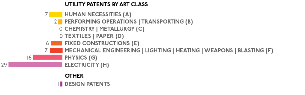
TOP LOCAL ASSIGNEES (NO. OF PATENTS)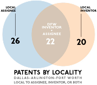
Texas Instruments Inc. (Dallas) 18
Futurewei Technologies, Inc. (Plano) 7
Geodynamics (Millsap) 2
Heatcraft Refrigeration Products LLC (Richardson) 2
STMicroelectronics, Inc. (Coppell) 2
Toyota Motor Engineering Manufacturing North America, Inc. (Plano) 2
UNASSIGNED 4
TOP LOCAL INVENTORS (NO. OF PATENTS)
Ashish Khandelwal (Irving) 2
Archana Venugopal (Dallas) 2
Luigi Colombo (Dallas) 2
SPEED: APPLICATION TO ISSUE (NO. OF DAYS)
![]() 250 days
250 days
Architectural lighting methods and apparatus
Patent No. 10180220
Assignee: Inception Innovations LLC (Southlake)
Inventor: Scott Eddins (Southlake)
![]() 2,708 days
2,708 days
Methods and systems for facilitating user access to media content programs included in a programming block
Patent No. 10182265
Assignee: Verizon Patent and Licensing Inc. (Basking Ridge, NJ)
Inventors: Brian F. Roberts (Dallas), Kristopher T. Frazier (Frisco)
Don’t miss Dallas Invents: Sign up for the Dallas Innovates e-newsletter. Patent information is provided by Joe Chiarella, founder of patent analytics company Patent Index and publisher of The Inventiveness Index.
For additional details on the patents granted below, search the USPTO Patent Full-Text and Image Database.
UTILITY PATENTS
H U M A N N E C E S S I T I E S
Micropellets of fine particle nutrients in snack food products
Patent No. 10178876
Inventor(s): Ajay Rajeshwar Bhaskar (Allen, TX), Chien-Seng Hwang (Frisco, TX), Deepali Palta (Dallas, TX), Eugenio Bortone (McKinney, TX), Jorge C. Morales-Alvarez (Plano, TX), Pierre Faa (Frisco, TX), Stefan K. Baier (Hartsdale, NY,
Assignee(s): Frito-Lay North America, Inc. (Plano, TX)
Law Firm: Carstens Cahoon, LLC (Local)
Application No., Date, Speed: 15273966 on 09/23/2016 (844 days app to issue)
Abstract: Nutritious granular materials of fine particle sizes agglomerated within versatile micropellets are useful for inserting significant amounts of nutritious properties into snack foods. Expandable micropellet-containing formulations provide for introduction of fine particle ingredients such as proteins, minerals and other components or desirable nutrients into food processing lines not typically amenable to the fine particle sizes. Micropellet-containing formulations may consist entirely of micropellets, or may contain an expandable starch such as, for example, corn meal, sheeted doughs, and expanded collet products onto which the micropellets may be basted. NULL
Refrigerated display cases with thermal-block doorframes
Patent No. 10178917
Inventor(s): Ajay Chidambaram Pillai Swornalatha (Kanyakumari, , IN), Rahul Gokhale (Dunwoody, GA), Revanth Muppala (Chennai, , IN), Saikiran Thoutam (Columbus, GA), Santosh Nerur (Suwanee, GA), Vinod Kunchala (Chennai, , IN)
Assignee(s): Heatcraft Refrigeration Products LLC (Richardson, TX)
Law Firm: Hubbard Johnston, PLLC (Local)
Application No., Date, Speed: 15264553 on 09/13/2016 (854 days app to issue)
Abstract: In a refrigerated display case having an interior volume that is accessed through a door panel being opened from a doorframe, a frame cover is included that may reduce condensation or the power required to avoid condensation on a door panel. The frame cover is formed of a non-metallic material that provides a thermal break. The frame cover may also be formed with air pockets to further enhance the thermal break. Moreover, it may be formed to attach with an interference fit and thereby avoid fasteners. Other embodiments and features are presented.
[A47F] SPECIAL FURNITURE, FITTINGS, OR ACCESSORIES FOR SHOPS, STOREHOUSES, BARS, RESTAURANTS, OR THE LIKE; PAYING COUNTERS
Apparatus and method for deploying an implantable device within the body
Patent No. 10179058
Inventor(s): Paul A. LaDuca (Little Elm, TX)
Assignee(s): Taheri LaDuca LLC (Santa Cruz, CA)
Law Firm: Levine Bagade Han LLP (1 non-local offices)
Application No., Date, Speed: 13619529 on 09/14/2012 (2314 days app to issue)
Abstract: The present invention provides devices and methods for fabricating and deploying an implantable device within the body. The invention is particularly suitable for delivering and deploying a stent, graft or stent graft device within a vessel or tubular structure within the body, particularly where the implant site involves two or more interconnecting vessels. The delivery and deployment system utilizes a plurality of strings which are releasably attached to the luminal ends of the implantable device.
[A61F] FILTERS IMPLANTABLE INTO BLOOD VESSELS; PROSTHESES; DEVICES PROVIDING PATENCY TO, OR PREVENTING COLLAPSING OF, TUBULAR STRUCTURES OF THE BODY, E.G. STENTS; ORTHOPAEDIC, NURSING OR CONTRACEPTIVE DEVICES; FOMENTATION; TREATMENT OR PROTECTION OF EYES OR EARS; BANDAGES, DRESSINGS OR ABSORBENT PADS; FIRST-AID KITS (dental prosthetics A61C) [2006.01]
Medical devices and methods for protecting a limb of a patient during a medical procedure
Patent No. 10179062
Inventor(s): J. Michael Putman (Dallas, TX), William W. Gardetto (Colleyville, TX)
Assignee(s): UNASSIGNED
Law Firm: Hubbard Johnston, PLLC (Local)
Application No., Date, Speed: 14673825 on 03/30/2015 (1387 days app to issue)
Abstract: Medical devices and methods are presented for protecting a limb, e.g., an arm, of a patient during a medical procedure. The medical devices and methods utilize a plurality of longitudinal sealed fluid pockets to thermally insulate and cushion an extremity of a limb. The plurality of longitudinal sealed fluid pockets is incorporated in a protective body that is shaped to wrap around the extremity when the medical device is deployed. The protective body has at least one access opening to provide access through the protective body to one or more corresponding portions of the extremity. Access panels may be formed into the protective body to allow portions of the extremity to be covered or uncovered and used with left or right limbs. Other devices and methods are presented.
[A61F] FILTERS IMPLANTABLE INTO BLOOD VESSELS; PROSTHESES; DEVICES PROVIDING PATENCY TO, OR PREVENTING COLLAPSING OF, TUBULAR STRUCTURES OF THE BODY, E.G. STENTS; ORTHOPAEDIC, NURSING OR CONTRACEPTIVE DEVICES; FOMENTATION; TREATMENT OR PROTECTION OF EYES OR EARS; BANDAGES, DRESSINGS OR ABSORBENT PADS; FIRST-AID KITS (dental prosthetics A61C) [2006.01]
Patient support with stand-up and sit features
Patent No. 10179077
Inventor(s): Tho Quang Thieu (Frisco, TX)
Assignee(s): Kreg Medical, Inc. (Melrose Park, IL)
Law Firm: Banner Witcoff, Ltd. (3 non-local offices)
Application No., Date, Speed: 14690387 on 04/18/2015 (1368 days app to issue)
Abstract: A bed is provided having a base frame, a patient support assembly connected to the base frame, and a tilt frame connected between the base frame and the patient support assembly. The tilt frame is rotatable adjacent the foot end of the bed to place the patient support assembly, including the head section, seat section and foot section thereof, in a generally vertical position to allow a patient to exit the bed in a standing orientation. The bed also has a foot board assembly connected to the foot section, the foot board assembly having a foot board separately moveable about a longitudinal axis of the bed toward the head end and the foot end of the bed.
[A61G] TRANSPORT, PERSONAL CONVEYANCES, OR ACCOMMODATION SPECIALLY ADAPTED FOR PATIENTS OR DISABLED PERSONS (appliances for aiding patients or disabled persons to walk A61H 3/00); OPERATING TABLES OR CHAIRS; CHAIRS FOR DENTISTRY; FUNERAL DEVICES (embalming corpses A01N 1/00)
Vision measurement and training system and method of operation thereof
Patent No. 10179081
Inventor(s): William R. Krenik (Richardson, TX)
Assignee(s): VITAL ART AND SCIENCE, LLC (Richardson, TX)
Law Firm: No Counsel
Application No., Date, Speed: 14928129 on 10/30/2015 (1173 days app to issue)
Abstract: One aspect of the disclosure provides a binocular viewing system. In one embodiment, the binocular viewing system includes a binocular viewer and a computer. The binocular viewer has left and right display screens and a variable focal depth optical subsystem located in an optical path between and separate from the display screens and a user when the user uses the binocular viewer. The computer is configured to provide control signals to the binocular viewer. The control signals are operable to place images on the left and right display screens and vary a focal depth of the variable focal depth optical subsystem. The images include a plurality of objects controlled by the variable focal depth optical subsystem to make at least one of the plurality of objects appear closer to the user and at least one of another of said plurality of objects appear farther away from the user.
[A61B] DIAGNOSIS; SURGERY; IDENTIFICATION (analysing biological material G01N, e.g. G01N 33/48)
Apparatus and system for an integrated exercise device
Patent No. 10179258
Inventor(s): Ranya Sabbagh (Frisco, TX)
Assignee(s): FIT TONED, LLC (Frisco, TX)
Law Firm: No Counsel
Application No., Date, Speed: 15891204 on 02/07/2018 (342 days app to issue)
Abstract: An apparatus, system, and method for using a portable exercise device. Various exercises are performable using the exercise device, including standing, sitting, and kneeling exercises that are particularly suited for resistance training. The portable exercise device includes a frame defining an empty space. The portable frame includes a top bar parallel to a bottom bar, and two side bars including a first side bar and a second side bar, as well as a first frame handle and a second frame handle. The first frame handle and the second frame handle are affixed substantially near an upper portion of the first side bar and the second side bar. The first frame handle and the second frame handle are in horizontal alignment with respect to each other. The portable exercise frame includes a set of attachment points distributed around the portable exercise frame configured to receive resistance bands.
[A63B] APPARATUS FOR PHYSICAL TRAINING, GYMNASTICS, SWIMMING, CLIMBING, OR FENCING; BALL GAMES; TRAINING EQUIPMENT (apparatus for passive exercising, massage A61H)
O P E R A T I O N S & T R A N S P O R T
Method and assembly for manufacturing door skin and wall with doorway
Patent No. 10179438
Inventor(s): Bryan Linington (Perth, , CA), Jacques Dionne (Saint-Andr-d”Argenteuil, , CA), Richard Gingras (Montreal, , CA), Sylvain Tessier (Fassett, , CA)
Assignee(s): Bell Helicopter Textron Inc. (Fort Worth, TX)
Law Firm: No Counsel
Application No., Date, Speed: 15273775 on 09/23/2016 (844 days app to issue)
Abstract: A method of manufacturing a door skin and a fuselage wall having a doorway and a member extending into the doorway for abutting the door includes placing a first sheet of uncured composite material on a mold plate to define the door and fuselage skin, disposing an insert over the first sheet overlapping a desired periphery of the door, placing a second sheet of uncured composite material on a peripheral portion of the insert and over the first sheet adjacent the peripheral portion of the insert to form the member, curing the sheets and bonding the sheets together adjacent the insert during the cure, removing the insert from between the sheets after cure, and separating the door skin from the wall skin after cure by moving a cutting tool through the first sheet and without penetrating the second sheet around the desired periphery of the door. An assembly for manufacturing the door skin and a fuselage wall is also discussed.
[B29C] SHAPING OR JOINING OF PLASTICS; SHAPING OF MATERIAL IN A PLASTIC STATE, NOT OTHERWISE PROVIDED FOR; AFTER-TREATMENT OF THE SHAPED PRODUCTS, e.g. REPAIRING (making preforms B29B 11/00; making laminated products by combining previously unconnected layers which become one product whose layers will remain together B32B 37/00-B32B 41/00) [4]
Using information obtained from fleet of vehicles for informational display and control of an autonomous vehicle
Patent No. 10179586
Inventor(s): Miles J. Johnson (Ann Arbor, MI)
Assignee(s): Toyota Motor Engineering Manufacturing North America, Inc. (Plano, TX)
Law Firm: Darrow Mustafa PC (2 non-local offices)
Application No., Date, Speed: 15234887 on 08/11/2016 (887 days app to issue)
Abstract: Described herein is an electronic control unit in an autonomous vehicle. The electronic control unit may comprise: a memory; and a processor coupled to the memory. The processor may be configured to: detect a first obstacle; determine first data related to the first obstacle; transmit the first data to a data aggregation service; receive, from the data aggregation service, second data related to a second obstacle; create a notification of the second obstacle; and deliver the notification to an interior of the autonomous vehicle.
[B60W] CONJOINT CONTROL OF VEHICLE SUB-UNITS OF DIFFERENT TYPE OR DIFFERENT FUNCTION; CONTROL SYSTEMS SPECIALLY ADAPTED FOR HYBRID VEHICLES; ROAD VEHICLE DRIVE CONTROL SYSTEMS FOR PURPOSES NOT RELATED TO THE CONTROL OF A PARTICULAR SUB-UNIT [2006.01]
F I X E D C O N S T R U C T I O N S
Roofing shingle system and shingles for use therein
Patent No. 10180001
Inventor(s): Olan Leitch (Bakersfield, CA)
Assignee(s): Building Materials Investment Corporation (Dallas, TX)
Law Firm: Venable LLP (7 non-local offices)
Application No., Date, Speed: 15369044 on 12/05/2016 (771 days app to issue)
Abstract: A laminated roofing shingle is disclosed comprising a posterior layer with tabs spaced apart by openings and an anterior layer with tabs spaced apart by openings, wherein the anterior layer is positioned offset from the posterior layer such that it partially overlaps the posterior layer in a manner such that the anterior layer does not entirely overlap the surface of the posterior tabs. A roofing system comprising a plurality of courses of the shingles is also disclosed as well as a method of manufacturing the shingle.
[E04D] ROOF COVERINGS; SKY-LIGHTS; GUTTERS; ROOF-WORKING TOOLS (coverings of outer walls by plaster or other porous material E04F 13/00)
Wall structure for a morphing structural member
Patent No. 10180027
Inventor(s): Danil V. Prokhorov (Canton, MI), Umesh N. Gandhi (Farmington Hills, MI), Yasuo Uehara (Ann Arbor, MI)
Assignee(s): Toyota Motor Engineering Manufacturing North America, Inc. (Plano, TX)
Law Firm: Darrow Mustafa PC (2 non-local offices)
Application No., Date, Speed: 15298240 on 10/20/2016 (817 days app to issue)
Abstract: A foldable dual-layered wall structure is positionable in a stowed condition and in a deployed condition. The wall structure includes a first foldable layer having at least a first pair of panels and a first joint rotatably connecting the panels of the at least a first pair of panels. A second foldable layer is positioned adjacent to the first foldable layer. The second foldable layer includes at least a second pair of panels and a second joint rotatably connecting the panels of the at least a second pair of panels. The wall structure is structured such that the first joint is positioned directly opposite a panel of the at least a second pair of panels and the second joint is positioned directly opposite a panel of the at least a first pair of panels when the wall structure is in the deployed condition.
[E04B] GENERAL BUILDING CONSTRUCTIONS; WALLS, e.g. PARTITIONS; ROOFS; FLOORS; CEILINGS; INSULATION OR OTHER PROTECTION OF BUILDINGS (border constructions of openings in walls, floors, or ceilings E06B 1/00)
Diamond cutting elements for drill bits seeded with HCP crystalline material
Patent No. 10180032
Inventor(s): Andrew David Murdock (Fort Worth, TX), John Martin Clegg (Fort Worth, TX), Matthew Douglas Mumma (Weatherford, TX), Neal Alan Bowden (Mansfield, TX), William Henry DuBose (Irving, TX)
Assignee(s): Ulterra Drilling Technologies, L.P. (Fort Worth, TX)
Law Firm: Hubbard Johnston, PLLC (Local)
Application No., Date, Speed: 13891040 on 05/09/2013 (2077 days app to issue)
Abstract: A polycrystalline diamond compact (PDC), which is attached or bonded to a substrate to form a cutter for a drill bit, is comprised of sintered polycrystalline diamond interspersed with a seed material which has a hexagonal close packed (HCP) crystalline structure. A region of the sintered polycrystalline diamond structure, near one or more of its working surfaces, which has been seeded with an HCP seed material prior to sintering, is leached to remove catalyst. Selectively seeding portions or regions of a sintered polycrystalline diamond structure permits differing leach rates to form leached regions with differing distances or depths and geometries.
[E21B] EARTH OR ROCK DRILLING (mining, quarrying E21C; making shafts, driving galleries or tunnels E21D); OBTAINING OIL, GAS, WATER, SOLUBLE OR MELTABLE MATERIALS OR A SLURRY OF MINERALS FROM WELLS [5]
Wellbore plug isolation system and method
Patent No. 10180037
Inventor(s): John T. Hardesty (Weatherford, TX), Michael D. Wroblicky (Weatherford, TX), Philip M. Snider (Tomball, TX)
Assignee(s): GEODYNAMICS, INC. (Millsap, TX)
Law Firm: Patent Portfolio Builders PLLC (4 non-local offices)
Application No., Date, Speed: 14721874 on 05/26/2015 (1330 days app to issue)
Abstract: A wellbore plug isolation system and method for positioning plugs to isolate fracture zones in a horizontal, vertical, or deviated wellbore is disclosed. The system/method includes a wellbore casing laterally drilled into a hydrocarbon formation, a wellbore setting tool (WST) that sets a large inner diameter (ID) restriction sleeve member (RSM), and a restriction plug element (RPE). The RPE includes a first composition and a second composition that changes phase or strength under wellbore conditions. After a stage is perforated, RPEs are deployed to isolate toe ward pressure communication. The second composition changes phase to create flow channels in the RPE during production. In an alternate system/method, the second composition changes phase or strength thereby deforming the RPE to reduce size and pass through the RSM”s. The RPEs are removed or left behind prior to initiating well production without the need for a milling procedure.
[E21B] EARTH OR ROCK DRILLING (mining, quarrying E21C; making shafts, driving galleries or tunnels E21D); OBTAINING OIL, GAS, WATER, SOLUBLE OR MELTABLE MATERIALS OR A SLURRY OF MINERALS FROM WELLS [5]
System and method of increasing reliability in high pressure switches
Patent No. 10180049
Inventor(s): Daniel S. Trafton (Kennedale, TX)
Assignee(s): UNASSIGNED
Law Firm: Damon R. Hickman Law Firm, P.C. (1 non-local offices)
Application No., Date, Speed: 15184296 on 06/16/2016 (943 days app to issue)
Abstract: A high pressure switch for controlling electrical signals between elements of a gun for perforating hydrocarbon wells. The switch uses mechanical energy from an explosion to change from one electrical path to a second electrical path. The switch has a piston that translates from the shockwave to electrical connect a firing pin to a conductive member while opening an electrical path from the piston to the firing pin.
[E21B] EARTH OR ROCK DRILLING (mining, quarrying E21C; making shafts, driving galleries or tunnels E21D); OBTAINING OIL, GAS, WATER, SOLUBLE OR MELTABLE MATERIALS OR A SLURRY OF MINERALS FROM WELLS [5]
Select fire switch control system and method
Patent No. 10180050
Inventor(s): John T Hardesty (Weatherford, TX)
Assignee(s): GEODYNAMICS, INC. (Millsap, TX)
Law Firm: Patent Portfolio Builders PLLC (4 non-local offices)
Application No., Date, Speed: 15221214 on 07/27/2016 (902 days app to issue)
Abstract: A select fire system and method for controlling operations in a gun string assembly includes perforating guns and switch subs mechanically connected in the gun string assembly. Each of the switch subs includes a switching element, input links and output links. The switch subs and perforating guns communicate with each other through the input and output links. The switching elements keep track of the state of the sub and switches states based on trigger conditions such as environment conditions, perforating gun conditions, or input conditions from surface.
[E21B] EARTH OR ROCK DRILLING (mining, quarrying E21C; making shafts, driving galleries or tunnels E21D); OBTAINING OIL, GAS, WATER, SOLUBLE OR MELTABLE MATERIALS OR A SLURRY OF MINERALS FROM WELLS [5]
M E C H A N I C A L E N G I N E E R I N G
LIGHTING | HEATING | WEAPONS | BLASTING
Apparatus for attaching a member to a core-stiffened structure and a combination thereof
Patent No. 10180151
Inventor(s): Carl A. May (Mansfield, TX), James D. Hethcock, Jr. (Colleyville, TX), John R. McCullough (Weatherford, TX), Ronald K. Cox (North Richland Hills, TX)
Assignee(s): Textron Innovations Inc. (Providence, RI)
Law Firm: No Counsel
Application No., Date, Speed: 14930176 on 11/02/2015 (1170 days app to issue)
Abstract: An apparatus for attaching a member to a honeycomb core-stiffened structure includes a body and one or more elements extending from the body configured to be adhesively bonded to one or more walls of a honeycomb core of the honeycomb core-stiffened structure. The apparatus further includes a fitting for attaching the member to the apparatus. A honeycomb core-stiffened structure includes a honeycomb core and an apparatus for attaching a member to the honeycomb core. The apparatus includes a body and one or more elements extending from the body configured to be adhesively bonded to one or more walls of the honeycomb core of the honeycomb core-stiffened structure. The apparatus further includes a fitting for attaching the member to the apparatus.
[F16B] DEVICES FOR FASTENING OR SECURING CONSTRUCTIONAL ELEMENTS OR MACHINE PARTS TOGETHER, e.g. NAILS, BOLTS, CIRCLIPS, CLAMPS, CLIPS OR WEDGES; JOINTS OR JOINTING (couplings for transmitting rotation F16D)
Bearing isolator seal with tapered static shutoff O-ring interface
Patent No. 10180189
Inventor(s): Jason Matthew Malocha (Scotts, MI), Joseph Charles Barker (Delton, MI), Robert Paul Bender (Bettendorf, IA)
Assignee(s): Flowserve Management Company (Irving, TX)
Law Firm: Maine Cernota Rardin (1 non-local offices)
Application No., Date, Speed: 15533129 on 12/08/2015 (1134 days app to issue)
Abstract: A bearing isolator seal having a shut off O-ring is tolerant of axial rotor-stator misalignment and provides an enhanced static seal while minimizing rotational wear. A tapered section of the stator is overlapped by the shut off O-ring. When the rotor is static there is no axial misalignment, and the shut off O-ring is pressed against the tapered section, forming an enhanced seal. During rotor rotation, increased axial misalignment moves the O-ring away from the tapered section, reducing rotational wear. The stator can extend horizontally beyond the tapered section and below the O-ring, so that if the rotor moves beyond a maximum misalignment, there is a ”line on line” fit between the stator and rotor. The bearing isolator seal can include labyrinth technology, and the tapered section can include a contour that allows the shutoff O-ring to drag along the surface of the tapered section with no hang-ups or binding.
[F16J] PISTONS; CYLINDERS; PRESSURE VESSELS IN GENERAL; SEALINGS
Architectural lighting methods and apparatus
Patent No. 10180220
Inventor(s): Scott Eddins (Southlake, TX)
Assignee(s): Inception Innovations, LLC (Southlake, TX)
Law Firm: No Counsel
Application No., Date, Speed: 15976742 on 05/10/2018 (250 days app to issue)
Abstract: An enclosed lighting unit for use with light strips is provided to enable installation of architectural lighting. The lighting unit has cooperating base and cover which are assembled by hand. The unit encloses a channel supporting the light strips which maintain a clearance distance between the light sources and the cover.
[F21S] NON-PORTABLE LIGHTING DEVICES; SYSTEMS THEREOF [7]
Quasi-sparse optical illumination
Patent No. 10180224
Inventor(s): Vikrant R. Bhakta (Dallas, TX)
Assignee(s): TEXAS INSTRUMENTS INCORPORATED (Dallas, TX)
Law Firm: No Counsel
Application No., Date, Speed: 15659600 on 07/25/2017 (539 days app to issue)
Abstract: In described examples, a DMD includes micromirrors. A first light source generates a first beam profile illuminating a first set of micromirrors of the DMD. A second light source generates a second beam profile illuminating a second set of micromirrors of the DMD. The first and second beam profiles partially overlap on at least some micromirrors of the DMD. The first light source is source-modulated independently of the second light source for adjusting power and brightness in response to a sensed driving condition. The micromirrors of the DMD are modulated in response to the sensed driving condition.
[F21S] NON-PORTABLE LIGHTING DEVICES; SYSTEMS THEREOF [7]
Walk-behind lawn mower universal lighting assembly
Patent No. 10180243
Inventor(s): Gary Blain Robertson (Arlington, TX)
Assignee(s): UNASSIGNED
Law Firm: Johnson | Dalal (no location found)
Application No., Date, Speed: 15894160 on 02/12/2018 (337 days app to issue)
Abstract: A universal lighting assembly detachably couples to a handle of a walk-behind lawn mower to illuminate areas in front of lawn mower. The assembly is universal, and thus operable with wide varieties of walk-behind lawn mowers. The lighting assembly comprises a light housing having a left side, a right side, and a front face with at least one LED. A left-side and a right-side arm project outwardly from the light housing. A concave clamp from each arm couples to the mower handles. A cylindrical drum couples to the left-side and right-side arms. The clamps and drum are stationary and not designed to rotate when clamped to the handle; thereby permitting rotation of the housing. A spring is housed within the cylindrical drum and with opposing ends coupled to left and right-side arms. The spring biases each arm in a longitudinal direction of cylindrical drum against lawn mower handles.
[F21V] FUNCTIONAL FEATURES OR DETAILS OF LIGHTING DEVICES OR SYSTEMS THEREOF; STRUCTURAL COMBINATIONS OF LIGHTING DEVICES WITH OTHER ARTICLES, NOT OTHERWISE PROVIDED FOR [7]
Expansion rack for compressor mounting
Patent No. 10180266
Inventor(s): Abdul Kader Peer Mohideen (Chennai, , IN), Ganesh Thokur (Chennai, , IN), Poly Joseph (Chennai, , IN)
Assignee(s): Heatcraft Refrigeration Products LLC (Richardson, TX)
Law Firm: Baker Botts L.L.P. (Local + 8 other metros)
Application No., Date, Speed: 15053206 on 02/25/2016 (1055 days app to issue)
Abstract: An apparatus includes a first metal beam and a mounting bracket. The first metal beam is arranged in a linearly horizontal direction and defines a plurality of first and second cavities along a top surface of the first metal beam. Each first cavity is of a first shape and is separated from another first cavity by a first distance. Each second cavity is of a second shape different from the first shape and is separated from another second cavity by a second distance greater than the first distance. The mounting bracket couples to the top surface of the first metal beam at a first mounting cavity of the plurality of second cavities and the top surface of the second metal beam at a second mounting cavity of the plurality of fourth cavities. The mounting bracket further couples to a compressor.
[F24F] AIR-CONDITIONING; AIR-HUMIDIFICATION; VENTILATION; USE OF AIR CURRENTS FOR SCREENING (removing dirt or fumes from areas where they are produced B08B 15/00; vertical ducts for carrying away waste gases from buildings E04F 17/02; tops for chimneys or ventilating shafts, terminals for flues F23L 17/02)
Secure personal item carrier weapon concealment compartment system
Patent No. 10180304
Inventor(s): Jian Liu (Plano, TX)
Assignee(s): UNASSIGNED
Law Firm: Braxton Perrone, PLLC (1 non-local offices)
Application No., Date, Speed: 15421263 on 01/31/2017 (714 days app to issue)
Abstract: A system and method for a secure weapon concealment compartment situated in a personal carrying item such as a purse, handbag, briefcase, backpack or luggage that allows a person to safely and efficiently carry, store and make available for use a weapon. The concealment compartment includes weapon securing having tapered holders or orifices formed to receive a weapon and provide safety against unintentional discharge of the weapon and resistive forces applied to a protective carrier of the weapon once stored to enable quick and effective withdrawal of the weapon from the concealment compartment.
[F41C] SMALLARMS, e.g. PISTOLS OR RIFLES (projecting missiles without use of explosive or combustible propellant charge F41B); ACCESSORIES THEREFOR [5]
P H Y S I C S
Robust heating, ventilation, and air conditioning communication channels
Patent No. 10180263
Inventor(s): Steve Charles Lazar (San Antonio, TX)
Assignee(s): Lennox Industries, Inc. (Richardson, TX)
Law Firm: Baker Botts L.L.P. (Local + 8 other metros)
Application No., Date, Speed: 14925550 on 10/28/2015 (1175 days app to issue)
Abstract: A heating, ventilation, and air conditioning (HVAC) communication method comprising generating, at a transmitter device, a primary signal and a secondary signal. Each of the signals comprise digital temperature data and digital humidity data. The secondary signal is a phase shifted representation of the primary signal. The HVAC communication method further comprises transmitting the primary signal and the secondary signal to a receiver device via a wireless link. The method continues by storing a look-up table that maps bit streams to temperature values and humidity values. The method continues by performing, at the receiver device, a comparison using the primary signal to execute error checking, and determining, at the receiver device, a temperature value and a humidity value using the look-up table based on the comparison.
[G05B] CONTROL OR REGULATING SYSTEMS IN GENERAL; FUNCTIONAL ELEMENTS OF SUCH SYSTEMS; MONITORING OR TESTING ARRANGEMENTS FOR SUCH SYSTEMS OR ELEMENTS (fluid-pressure actuators or systems acting by means of fluids in general F15B; valves per se F16K; characterised by mechanical features only G05G; sensitive elements, see the appropriate subclasses, e.g. G12B, subclasses of G01, H01; correcting units, see the appropriate subclasses, e.g. H02K)
Microelectromechanical gyroscope with rejection of disturbances and method of sensing an angular rate
Patent No. 10180324
Inventor(s): Carlo Valzasina (Gessate, , IT), Erik Daniel Svensson (Kista, , SE), Gert Ingvar Andersson (Lindome, , SE), Huantong Zhang (Coppell, TX), Matteo Fabio Brunetto (Garbagnate Milanese, , IT), Nils Einar Hedenstierna (Vastra Folunda, ,
Assignee(s): STMicroelectronics International NV (Plan les Ouates, , CH), STMicroelectronics S.r.l. (Agrate Brianza, , IT), STMicroelectronics, Inc. (Coppell, TX)
Law Firm: Seed Intellectual Property Law Group LLP (1 non-local offices)
Application No., Date, Speed: 15197414 on 06/29/2016 (930 days app to issue)
Abstract: A gyroscope includes a substrate, a first structure, a second structure and a third structure elastically coupled to the substrate and movable along a first axis. The first and second structure are arranged at opposite sides of the third structure with respect to the first axis A driving system is configured to oscillate the first and second structure along the first axis in phase with one another and in phase opposition with the third structure. The first, second and third structure are provided with respective sets of sensing electrodes, configured to be displaced along a second axis perpendicular to the first axis in response to rotations of the substrate about a third axis perpendicular to the first axis and to the second axis.
[G01C] MEASURING DISTANCES, LEVELS OR BEARINGS; SURVEYING; NAVIGATION; GYROSCOPIC INSTRUMENTS; PHOTOGRAMMETRY OR VIDEOGRAMMETRY (measuring liquid level G01F; radio navigation, determining distance or velocity by use of propagation effects, e.g. Doppler effect, propagation time, of radio waves, analogous arrangements using other waves G01S)
Dark current compensation for photon counting circuit
Patent No. 10180351
Inventor(s): Nagesh Surendranath (Karnataka, , IN), Rakul Viswanath (Tamil Nadu, , IN), Sandeep Kesrimal Oswal (Karnataka, , IN)
Assignee(s): TEXAS INSTRUMENTS INCORPORATED (Dallas, TX)
Law Firm: No Counsel
Application No., Date, Speed: 15373242 on 12/08/2016 (768 days app to issue)
Abstract: A circuit includes a charge sensitive amplifier (CSA) that includes an input to receive current from a photon sensor and generates an output signal that represents photons received by the sensor and dark current of the sensor. A control circuit generates a compensation signal to offset the dark current from the photon sensor at the input of the CSA. The control circuit couples feedback from the CSA to enable the compensation signal if the photon current received from the sensor is below a predetermined threshold. The control circuit decouples the feedback from the CSA to disable the compensation signal if the photon current received from the sensor is above the predetermined threshold.
[G01J] MEASUREMENT OF INTENSITY, VELOCITY, SPECTRAL CONTENT, POLARISATION, PHASE OR PULSE CHARACTERISTICS OF INFRA-RED, VISIBLE OR ULTRA-VIOLET LIGHT; COLORIMETRY; RADIATION PYROMETRY [2]
Systems and methods for performing cavity-enhanced absorption spectroscopy
Patent No. 10180394
Inventor(s): Purnendu Dasgupta (Arlington, TX)
Assignee(s): Board of Regents, The University of Texas System (Austin, TX)
Law Firm: Thomas | Horstemeyer, LLP (no location found)
Application No., Date, Speed: 15523642 on 11/06/2015 (1166 days app to issue)
Abstract: In one embodiment, a cavity-enhanced absorption spectroscopy system includes a cavity-enhanced absorbance cell in which a liquid sample can be provided for purposes of evaluation, the absorbance cell having diffusely reflective inner surfaces, a light source configured to emit light into the liquid sample within the absorbance cell, and a light detector configured to capture the light after it has passed through the liquid sample.
[G01J] MEASUREMENT OF INTENSITY, VELOCITY, SPECTRAL CONTENT, POLARISATION, PHASE OR PULSE CHARACTERISTICS OF INFRA-RED, VISIBLE OR ULTRA-VIOLET LIGHT; COLORIMETRY; RADIATION PYROMETRY [2]
Systems and methods of testing multiple dies
Patent No. 10180454
Inventor(s): Mahesh M. Mehendale (Bangalore, , IN), Rubin Ajit Parekhji (Bangalore, , IN), Vinod Menezes (Bangalore, , IN), Vipul K. Singhal (Bangalore, , IN)
Assignee(s): TEXAS INSTRUMENTS INCORPORATED (Dallas, TX)
Law Firm: No Counsel
Application No., Date, Speed: 15130429 on 04/15/2016 (1005 days app to issue)
Abstract: A method of testing a semiconductor wafer comprising a scribe line and a plurality of dies. The method includes implementing a first landing pad on the scribe line and implementing a first interconnect on the scribe line and between the first landing pad and a first cluster of the plurality of dies, thereby coupling the first landing pad to the first cluster of dies. The method also includes performing the testing of the first cluster of dies using automated test equipment (ATE) coupled to a probe tip by contacting the first landing pad with the probe tip and applying an ATE resource to the first cluster of dies.
[G01R] MEASURING ELECTRIC VARIABLES; MEASURING MAGNETIC VARIABLES (indicating correct tuning of resonant circuits H03J 3/12)
Terminal assemblies, end cap assemblies, and fiber optic enclosures incorporating the same
Patent No. 10180553
Inventor(s): David Kimondo Waruiru (Fort Worth, TX), Joshua David Henley (Keller, TX), Karyne Poissant Prevratil (Fort Worth, TX)
Assignee(s): Corning Research Development Corporation (Corning, NY)
Law Firm: No Counsel
Application No., Date, Speed: 15490319 on 04/18/2017 (637 days app to issue)
Abstract: Fiber optic enclosures, terminal assemblies, end cap assemblies, and methods of sealing fiber optic enclosures are disclosed. The terminal assembly of a fiber optic enclosure may include an input fiber sealing assembly and an output fiber sealing assembly. The input fiber sealing assembly may include an input fiber insert positioned in an input fiber channel of the cap body, an input fiber compression plate positioned in the input fiber channel, and an input fiber compression member for compressing the insert between the fiber compression plate and the base plate. The output fiber sealing assembly may include an output fiber insert positioned in the output fiber channel of the cap body, an output fiber compression plate positioned in the output fiber channel, and an output fiber compression member for compressing the insert between the fiber compression plate and the base plate.
[G02B] OPTICAL ELEMENTS, SYSTEMS, OR APPARATUS (G02F takes precedence; optical elements specially adapted for use in lighting devices or systems thereof F21V 1/00-F21V 13/00; measuring-instruments, see the relevant subclass of class G01, e.g. optical rangefinders G01C; testing of optical elements, systems, or apparatus G01M 11/00; spectacles G02C; apparatus or arrangements for taking photographs or for projecting or viewing them G03B; sound lenses G10K 11/30; electron and ion “optics” H01J; X-ray “optics” H01J, H05G 1/00; optical elements structurally combined with electric discharge tubes H01J 5/16, H01J 29/89, H01J 37/22; microwave “optics” H01Q; combination of optical elements with television receivers H04N 5/72; optical systems or arrangements in colour television systems H04N 9/00; heating arrangements specially adapted for transparent or reflecting areas H05B 3/84) [7]
Adaptive body bias for voltage regulator
Patent No. 10180694
Inventor(s): Angelo William Pereira (Allen, TX), Ashish Khandelwal (Irving, TX), Sujan Kundapur Manohar (Dallas, TX)
Assignee(s): TEXAS INSTRUMENTS INCORPORATED (Dallas, TX)
Law Firm: No Counsel
Application No., Date, Speed: 15655373 on 07/20/2017 (544 days app to issue)
Abstract: A voltage regulator (e.g., a low drop-out regulator) includes a pass transistor coupled to an input voltage node and an output voltage node. The voltage regulator also includes a drive transistor coupled to a control input of the pass transistor and a first resistor coupled between a source and a back gate of the drive transistor. The voltage regulator also includes a complementary to absolute temperature (CTAT) current generator circuit coupled to the resistor and configured to generate a CTAT current to bias the first resistor.
[G05F] SYSTEMS FOR REGULATING ELECTRIC OR MAGNETIC VARIABLES (regulating the timing or recurrence frequency of pulses in radar or radio navigation systems G01S; regulation of current or voltage, specially adapted for use in electronic time-pieces G04G 19/02; closed-loop systems for regulating non-electric variables by electric means G05D; regulating power supply of digital computers G06F 1/26; for obtaining desired operating characteristics of electromagnets with armatures H01F 7/18; regulating electric power distribution networks H02J; regulating the charging of batteries H02J 7/00; regulating of the output of static converters, e.g. switching regulators, H02M; regulation of the output of electric generators H02N, H02P 9/00; controlling transformers, reactors or choke coils H02P 13/00; regulating frequency response, gain, maximum output, amplitude or bandwidth of amplifiers H03G; regulating tuning of resonant circuits H03J; controlling generators of electronic oscillations or pulses H03L; regulating characteristics of transmission lines H04B; controlling electric light sources H05B 37/02, H05B 39/04, H05B 41/36; electric control of X-ray apparatus H05G 1/30) [5]
Dropout recovery with overshoot and inrush current reduction
Patent No. 10180695
Inventor(s): Simon M. Bikulcius (San Jose, CA)
Assignee(s): Texas Instruments Incorporated (Dallas, TX)
Law Firm: No Counsel
Application No., Date, Speed: 15956047 on 04/18/2018 (272 days app to issue)
Abstract: In a power management device, a hiccup mode is implemented by using, for example, a counter to count the number of cycles for which a current limiting event has occurred and forcing the power management device to hiccup when a certain number of current limiting events have been counted. A soft start circuit is typically employed to ramp up the output voltage when the power management device is turned back on. By resetting the soft start voltage to the feedback voltage of the load of the power management device upon the first detection of a current limiting event, hiccup can be avoided because resetting the soft start voltage to the feedback voltage will reduce the current in proceeding cycles thereby avoiding additional current limiting events.
[G05F] SYSTEMS FOR REGULATING ELECTRIC OR MAGNETIC VARIABLES (regulating the timing or recurrence frequency of pulses in radar or radio navigation systems G01S; regulation of current or voltage, specially adapted for use in electronic time-pieces G04G 19/02; closed-loop systems for regulating non-electric variables by electric means G05D; regulating power supply of digital computers G06F 1/26; for obtaining desired operating characteristics of electromagnets with armatures H01F 7/18; regulating electric power distribution networks H02J; regulating the charging of batteries H02J 7/00; regulating of the output of static converters, e.g. switching regulators, H02M; regulation of the output of electric generators H02N, H02P 9/00; controlling transformers, reactors or choke coils H02P 13/00; regulating frequency response, gain, maximum output, amplitude or bandwidth of amplifiers H03G; regulating tuning of resonant circuits H03J; controlling generators of electronic oscillations or pulses H03L; regulating characteristics of transmission lines H04B; controlling electric light sources H05B 37/02, H05B 39/04, H05B 41/36; electric control of X-ray apparatus H05G 1/30) [5]
Data storage device having internal tagging capabilities
Patent No. 10180788
Inventor(s): Judah Gamliel Hahn (Ofra, , IL), Orit Dor (Matan, , IL)
Assignee(s): SANDISK TECHNOLOGIES INC. (Plano, TX)
Law Firm: Patterson Sheridan, LLP (Local + 6 other metros)
Application No., Date, Speed: 15092296 on 04/06/2016 (1014 days app to issue)
Abstract: A data storage device includes a memory and a controller. The memory includes a first partition and a second partition. The controller includes a pattern detector that is configured to detect one or more tags in data from an access device to be stored in the first partition. The controller is configured to generate, in the second partition, one or more links to the data that is stored in the first partition, the one or more links organized according to metadata associated with the one or more tags.
[G06F] ELECTRIC DIGITAL DATA PROCESSING (computer systems based on specific computational models G06N)
Intelligent memory architecture for increased efficiency
Patent No. 10180803
Inventor(s): Alan Gatherer (Richardson, TX), Casen Hunger (Austin, TX), Hao Luan (Plano, TX), Hardik Jain (Austin, TX), Sriram Vishwanath (Austin, TX)
Assignee(s): Futurewei Technologies, Inc. (Plano, TX)
Law Firm: Schwegman Lundberg Woessner, P.A. (11 non-local offices)
Application No., Date, Speed: 14810895 on 07/28/2015 (1267 days app to issue)
Abstract: A method includes receiving a first request, from a first master core, to access data in one of a plurality of memory banks. It is determined whether an access to the data is stalled by virtue of a second request, from a second master core, to access the data in the one of the plurality of memory banks, the second request currently being serviced. In response to a determination that the access to the requested data is stalled, the first request is serviced by accessing data in one of a plurality of coding banks, each coding bank smaller in size than each memory bank.
[G06F] ELECTRIC DIGITAL DATA PROCESSING (computer systems based on specific computational models G06N)
Resource overprovisioning in a virtual machine environment
Patent No. 10180859
Inventor(s): Farid Khafizov (Plano, TX)
Assignee(s): Open Invention Network LLC (Durham, NC)
Law Firm: No Counsel
Application No., Date, Speed: 15708386 on 09/19/2017 (483 days app to issue)
Abstract: Systems, apparatuses, methods, and computer programs for overprovisioning resources are disclosed. Resource usage statistics may be gathered for a plurality of client virtual machines (”VMs”). Statistical characteristics of resource usage by the plurality of client VMs may be calculated. It may also be determined which of the plurality of client VMs requesting resources to allocate resources to, as well as an amount of the resources to allocate, in a given time slot based on the calculated statistical characteristics.
[G06F] ELECTRIC DIGITAL DATA PROCESSING (computer systems based on specific computational models G06N)
Methods and systems for depicting psychological analysis
Patent No. 10181158
Inventor(s): Edward Casteel Milner (Dallas, TX)
Assignee(s): ADDEPAR, INC. (Mountain View, CA)
Law Firm: Knobbe, Martens, Olson Bear, LLP (9 non-local offices)
Application No., Date, Speed: 14571984 on 12/16/2014 (1491 days app to issue)
Abstract: Systems and methods are presented for providing a psychological analysis of financial products in an investor”s financial portfolio. In some example embodiments, a method is presented. The method may include accessing, in a device comprising one or more processors, a psychometric data of a financial product, the psychometric data quantifying a decision-making tendency used in managing the financial product. The method may also include generating a psychological behavioral characteristic score of the financial product based on the accessed psychometric data, the psychological behavioral characteristic score indicating a degree to which the financial product exhibits a psychological characteristic relative to other financial products, generating an image of a graph that depicts the psychological behavioral characteristics score of the financial product relative to an axis that represents a range of degrees to which the psychological characteristic is exhibited by the other financial products, and causing display of the image of the graph.
[G06Q] DATA PROCESSING SYSTEMS OR METHODS, SPECIALLY ADAPTED FOR ADMINISTRATIVE, COMMERCIAL, FINANCIAL, MANAGERIAL, SUPERVISORY OR FORECASTING PURPOSES; SYSTEMS OR METHODS SPECIALLY ADAPTED FOR ADMINISTRATIVE, COMMERCIAL, FINANCIAL, MANAGERIAL, SUPERVISORY OR FORECASTING PURPOSES, NOT OTHERWISE PROVIDED FOR [2006.01]
Memory device write circuitry
Patent No. 10181344
Inventor(s): Harish N. Venkata (Allen, TX)
Assignee(s): Micron Technology, Inc. (Boise, ID)
Law Firm: Fletcher Yoder, P.C. (1 non-local offices)
Application No., Date, Speed: 15855485 on 12/27/2017 (384 days app to issue)
Abstract: Devices and methods include, for a memory device, generating a main input-output line signal on a main input-output line using driving circuitry. The main input-output line is coupled to multiple sensing amplifiers. Each of the sensing amplifiers each locally generate a local data line from the main data line. Each of the sensing amplifiers also includes multiple local sensing amplifiers that are selectively coupled to the generated local data line for overwriting data in the respective local sensing amplifiers.
[G11C] STATIC STORES (information storage based on relative movement between record carrier and transducer G11B; semiconductor devices for storage H01L, e.g. H01L 27/108-H01L 27/11597; pulse technique in general H03K, e.g. electronic switches H03K 17/00)
Cross-stratum optimization protocol
Patent No. 10181977
Inventor(s): Yangsong Xia (Richardson, TX), Young Lee (Plano, TX)
Assignee(s): Futurewei Technologies, Inc. (Plano, TX)
Law Firm: Conley Rose, P.C. (3 non-local offices)
Application No., Date, Speed: 14876313 on 10/06/2015 (1197 days app to issue)
Abstract: An apparatus comprising an application cross-stratum optimization (CSO) gateway (ACG) coupled to an application layer that handles a plurality of servers, a network CSO gateway (NCG) coupled to a network layer that handles a plurality of network nodes and configured to communicate with the ACG using a CSO protocol (CSOP), and a CSO interface established between the ACG and the NCG that enables the exchange of a plurality of CSOP messages to allow joint application-network resource allocation, provisioning, and optimization. Also disclosed is a network apparatus implemented method comprising sending a user profile from a user plane to an application plane, sending an application profile from the application plane to a network plane via a CSO interface between an ACG and a NCG, and sending network capability information from the network plane to the application plane via the CSO interface.
[G06F] ELECTRIC DIGITAL DATA PROCESSING (computer systems based on specific computational models G06N)
Decentralized, hierarchical, and overlay-driven mobility support architecture for information-centric networks
Patent No. 10182091
Inventor(s): Aytac Azgin (Santa Clara, CA), Guoqiang Wang (Santa Clara, CA), Ravishankar Ravindran (San Ramon, CA)
Assignee(s): Futurewei Technologies, Inc. (Plano, TX)
Law Firm: Schwegman Lundberg Woessner, P.A. (11 non-local offices)
Application No., Date, Speed: 15159033 on 05/19/2016 (971 days app to issue)
Abstract: An anchor server in an information-centric network (ICN) receives registration and deregistration requests from one or more producers in the ICN. In response to a producer initially registering, the anchor server stores records associating the producer with content available from the producer via a first point of attachment. In response to the producer deregistering, the records are marked as deactivated. While the records are deactivated, requests for the content from consumers may be queued. In response to the producer reregistering as being connected to the ICN via a second point of attachment, the queued requests are forwarded to the producer via the second point of attachment.
[G06F] ELECTRIC DIGITAL DATA PROCESSING (computer systems based on specific computational models G06N)
Methods and systems for facilitating user access to media content programs included in a programming block
Patent No. 10182265
Inventor(s): Brian F. Roberts (Dallas, TX), Kristopher T. Frazier (Frisco, TX)
Assignee(s): Verizon Patent and Licensing Inc. (Basking Ridge, NJ)
Law Firm: No Counsel
Application No., Date, Speed: 13211812 on 08/17/2011 (2708 days app to issue)
Abstract: An exemplary method includes a media content presentation system detecting an access event initiated by a user and performed by a media content processing subsystem with respect to a media content program during a time period associated with a provider-scheduled presentation of the media content program, identifying a programming block of which the media content program is a part, determining that the user has failed to direct the media content processing subsystem to perform an additional access event with respect to one or more additional media content programs that are also a part of the programming block during a time period associated with a provider-scheduled presentation of the one or more additional media content programs, and facilitating, in response to the determining, access by the user to the one or more additional media content programs included in the programming block. Corresponding methods and systems are also disclosed.
[G06F] ELECTRIC DIGITAL DATA PROCESSING (computer systems based on specific computational models G06N)
E L E C T R I C I T Y
Electronic sensors with sensor die in package structure cavity
Patent No. 10179730
Inventor(s): Barry Jon Male (West Granby, CT), Benjamin Cook (Addison, TX), Robert Alan Neidorff (Bedford, NH), Steve Kummerl (Carrollton, TX)
Assignee(s): TEXAS INSTRUMENTS INCORPORATED (Dallas, TX)
Law Firm: No Counsel
Application No., Date, Speed: 15372565 on 12/08/2016 (768 days app to issue)
Abstract: Disclosed examples include sensor apparatus and integrated circuits having a package structure with an internal cavity and an opening that connects of the cavity with an ambient condition of an exterior of the package structure, and an electronic sensor structure mechanically supported by wires in the cavity and including a sensing surface exposed to the cavity to sense the ambient condition of an exterior of the package structure.
[H01L] SEMICONDUCTOR DEVICES; ELECTRIC SOLID STATE DEVICES NOT OTHERWISE PROVIDED FOR (use of semiconductor devices for measuring G01; resistors in general H01C; magnets, inductors, transformers H01F; capacitors in general H01G; electrolytic devices H01G 9/00; batteries, accumulators H01M; waveguides, resonators, or lines of the waveguide type H01P; line connectors, current collectors H01R; stimulated-emission devices H01S; electromechanical resonators H03H; loudspeakers, microphones, gramophone pick-ups or like acoustic electromechanical transducers H04R; electric light sources in general H05B; printed circuits, hybrid circuits, casings or constructional details of electrical apparatus, manufacture of assemblages of electrical components H05K; use of semiconductor devices in circuits having a particular application, see the subclass for the application) [2]
Lead frame assembly
Patent No. 10181435
Inventor(s): Makoto Shibuya (Beppu, , JP)
Assignee(s): TEXAS INSTRUMENTS INCORPORATED (Dallas, TX)
Law Firm: No Counsel
Application No., Date, Speed: 14930142 on 11/02/2015 (1170 days app to issue)
Abstract: A leadframe assembly includes a leadframe having a die attach pad and a first plurality of leads. A first generally sine wave-shaped wire having a first end and a second end has a first end of thereof attached to a first one of the first plurality of leads and the second end thereof attached to a second one of the first plurality of leads. A method of making a leadframe assembly includes forming an inductor on a leadframe by bending a first wire into a generally sine wave-shaped configuration and attaching the first wire to a first set of leads of the leadframe.
[H01L] SEMICONDUCTOR DEVICES; ELECTRIC SOLID STATE DEVICES NOT OTHERWISE PROVIDED FOR (use of semiconductor devices for measuring G01; resistors in general H01C; magnets, inductors, transformers H01F; capacitors in general H01G; electrolytic devices H01G 9/00; batteries, accumulators H01M; waveguides, resonators, or lines of the waveguide type H01P; line connectors, current collectors H01R; stimulated-emission devices H01S; electromechanical resonators H03H; loudspeakers, microphones, gramophone pick-ups or like acoustic electromechanical transducers H04R; electric light sources in general H05B; printed circuits, hybrid circuits, casings or constructional details of electrical apparatus, manufacture of assemblages of electrical components H05K; use of semiconductor devices in circuits having a particular application, see the subclass for the application) [2]
Three-dimensional memory device having L-shaped word lines and methods of making the same
Patent No. 10181442
Inventor(s): Akira Takahashi (Yokkaichi, , JP), Haruki Urata (Yokkaichi, , JP), Kazuto Watanabe (Yokkaichi, , JP), Michiaki Sano (Yokkaichi, , JP)
Assignee(s): SANDISK TECHNOLOGIES LLC (Addison, TX)
Law Firm: The Marbury Law Group PLLC (3 non-local offices)
Application No., Date, Speed: 15826796 on 11/30/2017 (411 days app to issue)
Abstract: A three-dimensional memory device includes an alternating stack of L-shaped insulating layers and L-shaped electrically conductive layers located over a top surface of a substrate, such that each of the L-shaped insulating layers and the L-shaped electrically conductive layers includes a respective horizontally-extending portion and a respective non-horizontally-extending portion, memory stack structures extending through a memory array region of the alternating stack that includes the horizontally-extending portions of the L-shaped electrically conductive layers, such that each of the memory stack structures includes a memory film and a vertical semiconductor channel, dielectric spacers non-horizontally extending between neighboring pairs of a non-horizontally-extending portion of an L-shaped insulating layer and a non-horizontally-extending portion of an L-shaped electrically conductive layer, and contact via structures that contact a respective one of the non-horizontally-extending portions of the L-shaped electrically conductive layers.
[H01L] SEMICONDUCTOR DEVICES; ELECTRIC SOLID STATE DEVICES NOT OTHERWISE PROVIDED FOR (use of semiconductor devices for measuring G01; resistors in general H01C; magnets, inductors, transformers H01F; capacitors in general H01G; electrolytic devices H01G 9/00; batteries, accumulators H01M; waveguides, resonators, or lines of the waveguide type H01P; line connectors, current collectors H01R; stimulated-emission devices H01S; electromechanical resonators H03H; loudspeakers, microphones, gramophone pick-ups or like acoustic electromechanical transducers H04R; electric light sources in general H05B; printed circuits, hybrid circuits, casings or constructional details of electrical apparatus, manufacture of assemblages of electrical components H05K; use of semiconductor devices in circuits having a particular application, see the subclass for the application) [2]
SRAM layout for double patterning
Patent No. 10181474
Inventor(s): James Walter Blatchford (Richardson, TX)
Assignee(s): TEXAS INSTRUMENTS INCORPORATED (Dallas, TX)
Law Firm: No Counsel
Application No., Date, Speed: 13622971 on 09/19/2012 (2309 days app to issue)
Abstract: An integrated circuit with a SAR SRAM cell with power routed in metal-1. An integrated circuit with a SAR SRAM cell that has power routed in Metal-1 and has metal-1 and metal-2 integrated circuit and SAR SRAM cell patterns which are DPT compatible. A process of forming an integrated circuit with a SAR SRAM cell with DPT compatible integrated circuit and SAR SRAM cell metal-1 and metal-2 patterns.
[H01L] SEMICONDUCTOR DEVICES; ELECTRIC SOLID STATE DEVICES NOT OTHERWISE PROVIDED FOR (use of semiconductor devices for measuring G01; resistors in general H01C; magnets, inductors, transformers H01F; capacitors in general H01G; electrolytic devices H01G 9/00; batteries, accumulators H01M; waveguides, resonators, or lines of the waveguide type H01P; line connectors, current collectors H01R; stimulated-emission devices H01S; electromechanical resonators H03H; loudspeakers, microphones, gramophone pick-ups or like acoustic electromechanical transducers H04R; electric light sources in general H05B; printed circuits, hybrid circuits, casings or constructional details of electrical apparatus, manufacture of assemblages of electrical components H05K; use of semiconductor devices in circuits having a particular application, see the subclass for the application) [2]
Graphene FET with graphitic interface layer at contacts
Patent No. 10181516
Inventor(s): Archana Venugopal (Dallas, TX), Luigi Colombo (Dallas, TX)
Assignee(s): TEXAS INSTRUMENTS INCORPORATED (Dallas, TX)
Law Firm: No Counsel
Application No., Date, Speed: 15865795 on 01/09/2018 (371 days app to issue)
Abstract: A method for forming a graphene FET includes providing a graphene layer having a surface. A first metal layer having a work function 4.3 eV is deposited on the graphene surface. The first metal layer is oxidized to form a first metal oxide layer. The first metal oxide layer is etched to provide open surface contact regions including a first and a second region of the graphene layer for providing a graphene surface source and drain contact. A second metal layer is deposited including a second metal layer portion providing a source with a source contact over the graphene surface source contact and a second metal layer portion providing a drain with a drain contact over the graphene surface drain contact. A grown-in graphitic interface layer is formed at an interface between the source contact and graphene surface source contact and the drain contact and graphene surface drain contact.
[H01L] SEMICONDUCTOR DEVICES; ELECTRIC SOLID STATE DEVICES NOT OTHERWISE PROVIDED FOR (use of semiconductor devices for measuring G01; resistors in general H01C; magnets, inductors, transformers H01F; capacitors in general H01G; electrolytic devices H01G 9/00; batteries, accumulators H01M; waveguides, resonators, or lines of the waveguide type H01P; line connectors, current collectors H01R; stimulated-emission devices H01S; electromechanical resonators H03H; loudspeakers, microphones, gramophone pick-ups or like acoustic electromechanical transducers H04R; electric light sources in general H05B; printed circuits, hybrid circuits, casings or constructional details of electrical apparatus, manufacture of assemblages of electrical components H05K; use of semiconductor devices in circuits having a particular application, see the subclass for the application) [2]
Graphene heterolayers for electronic applications
Patent No. 10181521
Inventor(s): Archana Venugopal (Dallas, TX), Benjamin Stassen Cook (Rockwall, TX), Luigi Colombo (Dallas, TX), Robert Reid Doering (Garland, TX)
Assignee(s): TEXAS INSTRUMENTS INCORPORATED (Dallas, TX)
Law Firm: No Counsel
Application No., Date, Speed: 15437818 on 02/21/2017 (693 days app to issue)
Abstract: A microelectronic device includes an electrical conductor which includes a graphene heterolayer. The graphene heterolayer includes a plurality of alternating layers of graphene and barrier material. Each layer of the graphene has one to two atomic layers of graphene. Each layer of the barrier material has one to three layers of hexagonal boron nitride, cubic boron nitride, and/or aluminum nitride. The layers of graphene and the layers of barrier material may be continuous, or may be disposed in nanoparticles of a nanoparticle film.
[H01L] SEMICONDUCTOR DEVICES; ELECTRIC SOLID STATE DEVICES NOT OTHERWISE PROVIDED FOR (use of semiconductor devices for measuring G01; resistors in general H01C; magnets, inductors, transformers H01F; capacitors in general H01G; electrolytic devices H01G 9/00; batteries, accumulators H01M; waveguides, resonators, or lines of the waveguide type H01P; line connectors, current collectors H01R; stimulated-emission devices H01S; electromechanical resonators H03H; loudspeakers, microphones, gramophone pick-ups or like acoustic electromechanical transducers H04R; electric light sources in general H05B; printed circuits, hybrid circuits, casings or constructional details of electrical apparatus, manufacture of assemblages of electrical components H05K; use of semiconductor devices in circuits having a particular application, see the subclass for the application) [2]
FinFet having dual vertical spacer and method of manufacturing the same
Patent No. 10181527
Inventor(s): Mark Rodder (Dallas, TX)
Assignee(s): Samsung Electronics Co., Ltd. (Suwon-si, , KR)
Law Firm: Lewis Roca Rothgerber Christie LLP (6 non-local offices)
Application No., Date, Speed: 15169621 on 05/31/2016 (959 days app to issue)
Abstract: A field effect transistor (FET) structure includes: a gate; a first spacer having a first dielectric constant at a first region adjacent to the gate; and a second spacer having a second dielectric constant that is greater than the first dielectric constant at a second region adjacent to the gate.
[H01L] SEMICONDUCTOR DEVICES; ELECTRIC SOLID STATE DEVICES NOT OTHERWISE PROVIDED FOR (use of semiconductor devices for measuring G01; resistors in general H01C; magnets, inductors, transformers H01F; capacitors in general H01G; electrolytic devices H01G 9/00; batteries, accumulators H01M; waveguides, resonators, or lines of the waveguide type H01P; line connectors, current collectors H01R; stimulated-emission devices H01S; electromechanical resonators H03H; loudspeakers, microphones, gramophone pick-ups or like acoustic electromechanical transducers H04R; electric light sources in general H05B; printed circuits, hybrid circuits, casings or constructional details of electrical apparatus, manufacture of assemblages of electrical components H05K; use of semiconductor devices in circuits having a particular application, see the subclass for the application) [2]
Area-efficient active-FET ESD protection circuit
Patent No. 10181721
Inventor(s): Farzan Farbiz (Royal Oak, MI), Muhammad Yusuf Ali (Allen, TX), Xianzhi Dai (Shanghai, , CN)
Assignee(s): TEXAS INSTRUMENTS INCORPORATED (Dallas, TX)
Law Firm: No Counsel
Application No., Date, Speed: 15434280 on 02/16/2017 (698 days app to issue)
Abstract: An electrostatic discharge (ESD) protection circuit includes a high power supply rail (VDD) and a low power supply rail (VSS). The ESD protection circuit further includes an active shunt transistor coupled between VDD and VSS. The active shunt transistor includes a gate. The ESD protection circuit also includes a sensing transistor connected between an input/output (I/O) pad and the gate of the active shunt transistor. If an ESD stress event occurs on the I/O pad or on a VDD pad, the sensing transistor is caused to be turned ON thereby permitting a voltage on the I/O or VDD pad experiencing the ESD stress event to turn ON the active shunt transistor in turn causing ESD current to flow from the pad experiencing the ESD event, through VDD, and through the active shunt transistor to VSS.
[H02H] EMERGENCY PROTECTIVE CIRCUIT ARRANGEMENTS (indicating or signalling undesired working conditions G01R, e.g. G01R 31/00, G08B; locating faults along lines G01R 31/08; emergency protective devices H01H)
Circuit and architecture for a demodulator for a wireless power transfer system and method therefor
Patent No. 10181754
Inventor(s): Ashish Khandelwal (Irving, TX), Bharath B. Kannan (Merimack, NH), Joseph M. Khayat (Bedford, NH), Robert A. Neidorff (Bedford, NH), Yipeng Su (Blacksburg, VA)
Assignee(s): Texas Instruments Incorporated (Dallas, TX)
Law Firm: No Counsel
Application No., Date, Speed: 15174601 on 06/06/2016 (953 days app to issue)
Abstract: A primary side wireless power transmitter inductively couplable to a secondary side wireless power receiver for supplying power to the wireless power receiver for receiving communications from the secondary side wireless power receiver through the inductive coupling comprises a primary side tank circuit receiving a signal on from the secondary side wireless power receiver. A phase delay or time delay circuit generates a fixed delay clock signal. A sample and hold circuit samples a tank circuit voltage utilizing the fixed phase or time delayed clock signal. A comparator is coupled to an output of the sample and hold circuit for extracting data or commands from the signal stream. A method of operating a primary side wireless transmitter inductively coupled to a secondary side wireless power receiver for supplying power to the wireless power receiver to power a load coupled to the receiver is also disclosed.
[H02J] CIRCUIT ARRANGEMENTS OR SYSTEMS FOR SUPPLYING OR DISTRIBUTING ELECTRIC POWER; SYSTEMS FOR STORING ELECTRIC ENERGY (power supply circuits for apparatus for measuring X-radiation, gamma radiation, corpuscular radiation or cosmic radiation G01T 1/175; electric power supply circuits specially adapted for use in electronic time-pieces with no moving parts G04G 19/00; for digital computers G06F 1/18; for discharge tubes H01J 37/248; circuits or apparatus for the conversion of electric power, arrangements for control or regulation of such circuits or apparatus H02M; interrelated control of several motors, control of a prime-mover/generator combination H02P; control of high-frequency power H03L; additional use of power line or power network for transmission of information H04B)
Baluns for RF signal conversion and impedance matching
Patent No. 10181834
Inventor(s): Petteri Litmanen (Richardson, TX), Richard Francis Taylor (Campbell, CA), Siraj Akhtar (Richardson, TX)
Assignee(s): TEXAS INSTRUMENTS INCORPORATED (Dallas, TX)
Law Firm: No Counsel
Application No., Date, Speed: 15672070 on 08/08/2017 (525 days app to issue)
Abstract: In described examples of a magnetically coupled structure on a substrate with an integrated circuit device, the structure includes a first coil in a differential configuration, a second coil located above the first coil in a generally stacked configuration, and a center tap connection to a winding of the second coil. The first coil includes a first differential terminal, a second differential terminal, and metal windings of the first coil. The first coil”s metal windings form a continuous spiral electrical path between the first and second differential terminals. The first coil”s metal windings include turns and crossing connections between the turns. The turns are fabricated in an integrated circuit metal wiring level, and the crossing connections are fabricated in at least one metal level other than the metal wiring level containing the turns. The center tap is positioned to create a balanced structure.
[H01L] SEMICONDUCTOR DEVICES; ELECTRIC SOLID STATE DEVICES NOT OTHERWISE PROVIDED FOR (use of semiconductor devices for measuring G01; resistors in general H01C; magnets, inductors, transformers H01F; capacitors in general H01G; electrolytic devices H01G 9/00; batteries, accumulators H01M; waveguides, resonators, or lines of the waveguide type H01P; line connectors, current collectors H01R; stimulated-emission devices H01S; electromechanical resonators H03H; loudspeakers, microphones, gramophone pick-ups or like acoustic electromechanical transducers H04R; electric light sources in general H05B; printed circuits, hybrid circuits, casings or constructional details of electrical apparatus, manufacture of assemblages of electrical components H05K; use of semiconductor devices in circuits having a particular application, see the subclass for the application) [2]
Ring amplitude measurement and mitigation
Patent No. 10181847
Inventor(s): Nathan Schemm (Rowlett, TX), Rajarshi Mukhopadhyay (Allen, TX), Rajdeep Bondade (Richardson, TX)
Assignee(s): TEXAS INSTRUMENTS INCORPORATED (Dallas, TX)
Law Firm: No Counsel
Application No., Date, Speed: 15636365 on 06/28/2017 (566 days app to issue)
Abstract: An apparatus includes a voltage divider circuit including a plurality of series-connected capacitors and including an input terminal of one of the capacitors configured to receive a first voltage from a switch, and a ring node comprising the connection between at least two of the series-connected capacitors. The apparatus further includes a negative clamp circuit coupled to the ring node of the voltage divider circuit and a bias voltage node. The bias voltage node is configured to receive a bias voltage and responsive to a ring voltage on the ring node being less than the bias voltage, the negative clamp circuit is configured to clamp the ring voltage at a first threshold voltage. The apparatus also includes a peak detector circuit coupled to the ring node of the voltage divider circuit and configured to detect a peak amplitude of the ring voltage. The apparatus further includes a switch driver coupled to the peak detector circuit and configured to adjust a control signal to the switch responsive to the detected peak amplitude.
[H03K] PULSE TECHNIQUE (measuring pulse characteristics G01R; modulating sinusoidal oscillations with pulses H03C; transmission of digital information H04L; discriminator circuits detecting phase difference between two signals by counting or integrating cycles of oscillation H03D 3/04; automatic control, starting, synchronisation or stabilisation of generators of electronic oscillations or pulses where the type of generator is irrelevant or unspecified H03L; coding, decoding or code conversion, in general H03M) [4]
Analog-to-digital converter error correction
Patent No. 10181857
Inventor(s): Dimitar T. Trifonov (Vail, AZ)
Assignee(s): TEXAS INSTRUMENTS INCORPORATED (Dallas, TX)
Law Firm: No Counsel
Application No., Date, Speed: 15808444 on 11/09/2017 (432 days app to issue)
Abstract: An analog-to-digital converter includes an integrator, a single comparator, a successive approximation result register, and correction circuitry. The comparator is coupled to an output of the integrator. The successive approximation result register is coupled to an output of the comparator. The correction circuitry is configured to determine whether a sum of a reference voltage and an output voltage of the integrator changes an output of the comparator. The correction circuitry is also configured to, responsive to the sum of the reference voltage and the output of the integrator not changing the output of the comparator, add twice the reference voltage to the output of the integrator to produce a bit value at the output of the comparator, and select a bit value to be loaded into the successive approximation result register based on the bit value at the output of the comparator.
[H03M] CODING, DECODING OR CODE CONVERSION, IN GENERAL (using fluidic means F15C 4/00; optical analogue/digital converters G02F 7/00; coding, decoding or code conversion, specially adapted for particular applications, see the relevant subclasses, e.g. G01D, G01R, G06F, G06T, G09G, G10L, G11B, G11C, H04B, H04L, H04M, H04N; ciphering or deciphering for cryptography or other purposes involving the need for secrecy G09C) [4]
Reference voltage control circuit for a two-step flash analog-to-digital converter
Patent No. 10181861
Inventor(s): Jafar Sadique Kaviladath (Kozhikode, , IN), Neeraj Shrivastava (Bengaluru, , IN)
Assignee(s): TEXAS INSTRUMENTS INCORPORATED (Dallas, TX)
Law Firm: No Counsel
Application No., Date, Speed: 15883623 on 01/30/2018 (350 days app to issue)
Abstract: A circuit, which is usable in a flash analog-to-digital converter, includes a first switch configured to provide a first reference voltage to a first reference node responsive to a first control signal and a second switch configured to provide the first reference voltage to a second reference node responsive to a second control signal. A third switch is coupled to the first switch and is configured to provide a second reference voltage to the first reference node responsive to a clock signal. Further, a fourth switch is coupled to the second switch and configured to provide the second reference voltage to the second reference node responsive to the clock signal.
[H03M] CODING, DECODING OR CODE CONVERSION, IN GENERAL (using fluidic means F15C 4/00; optical analogue/digital converters G02F 7/00; coding, decoding or code conversion, specially adapted for particular applications, see the relevant subclasses, e.g. G01D, G01R, G06F, G06T, G09G, G10L, G11B, G11C, H04B, H04L, H04M, H04N; ciphering or deciphering for cryptography or other purposes involving the need for secrecy G09C) [4]
Parameterizable bandpass delta-sigma modulator
Patent No. 10181862
Inventor(s): Mark B. Yeary (Krum, TX)
Assignee(s): RAYTHEON COMPANY (Waltham, MA)
Law Firm: Lewis Roca Rothgerber Christie LLP (6 non-local offices)
Application No., Date, Speed: 15879024 on 01/24/2018 (356 days app to issue)
Abstract: A delta-sigma modulator (DSM) includes: a first summation circuit coupled to an input signal for subtracting an error feedback signal from the input signal; a tunable signal transfer function coupled to the first summation circuit for setting a desired pole in a frequency response of the DSM; a second summation circuit coupled to the tunable signal transfer function for adding a noise transfer function to an output of the tunable signal transfer function; and a quantizer coupled to the second summation circuit for quantizing an output of the second summation circuit to generate an output of the DSM. The output of the DSM is used as feedback to the first summation circuit as the error feedback signal, and the tunable signal transfer function is dynamically tuned to allow selecting and tuning a center frequency and a bandwidth of the DSM.
[H03M] CODING, DECODING OR CODE CONVERSION, IN GENERAL (using fluidic means F15C 4/00; optical analogue/digital converters G02F 7/00; coding, decoding or code conversion, specially adapted for particular applications, see the relevant subclasses, e.g. G01D, G01R, G06F, G06T, G09G, G10L, G11B, G11C, H04B, H04L, H04M, H04N; ciphering or deciphering for cryptography or other purposes involving the need for secrecy G09C) [4]
Enhanced powerline communication methods and devices
Patent No. 10181873
Inventor(s): James D. Allen (La Grange, KY), Oleg Logvinov (East Brunswick, NJ)
Assignee(s): STMICROELECTRONICS, INC. (Coppell, TX)
Law Firm: Seed IP Law Group LLP (1 non-local offices)
Application No., Date, Speed: 14980641 on 12/28/2015 (1114 days app to issue)
Abstract: A powerline communication system includes a plurality of rail segments. Each of the rail segments is electrically isolated from other rail segments, and each receives power from a rail segment power supply. At least one cart operates on the rail segments. The cart has a powerline communications controller. Each rail segment has a current state defined by how many and which carts are operating on the rail segment. A central coordinator is coupled to each rail segment and configured to execute a channel estimation using a sounding protocol on its rail segment. The central coordinators store tone maps associated with the possible states of its rail segment, and possibly its adjacent rail segment. A main controller communicates with each central coordinator to direct the state and future state of its segment so that tone maps and network keys can be managed by the CCo in advance of an imminent state change. The main controller or CCo may also execute channel estimation using a sounding protocol and cause updated tone map information to be sent to each central coordinator in advance of an imminent state change.
[H04B] TRANSMISSION [4]
Method and apparatus for optical wireless architecture
Patent No. 10181909
Inventor(s): Jianjun Yu (Princeton, NJ)
Assignee(s): ZTE (USA) Inc. (Richardson, TX)
Law Firm: Drinker Biddle Reath LLP (4 non-local offices)
Application No., Date, Speed: 13284561 on 10/28/2011 (2636 days app to issue)
Abstract: Embodiments of the present invention pertain to optical wireless architecture. More particularly, certain embodiments of the invention pertain to a novel method and apparatus to generate millimeter-wave signals with simple and/or low cost architecture. Simple millimeter-wave generation and dispersion-tolerant transmission is based on photonic mixing of two free-running lightwaves and self-mixing down-conversion. More particularly, heterodyne mixing of two free run lightwaves is achieved, wherein one lightwave is modulated by an external modulator driven by electrical data as one of the side-bands of a millimeter-wave signal. Optical to electrical conversion is performed and the millimeter-wave signal is broadcasted by a high-frequency antenna to a receiving side having a local oscillator with self-mixing architecture to down-convert the radio frequency to its baseband form.
[H04B] TRANSMISSION [4]
Configuration sub-system for telecommunication systems
Patent No. 10181911
Inventor(s): Ahmed H. Hmimy (Richardson, TX), Matthew Thomas Melester (McKinney, TX)
Assignee(s): Andrew Wireless Systems GmbH (Buchdorf, , DE)
Law Firm: Fogg Powers LLC (1 non-local offices)
Application No., Date, Speed: 14448080 on 07/31/2014 (1629 days app to issue)
Abstract: Certain aspects are directed to a configuration sub-system for telecommunication systems. The configuration sub-system can include a test signal generator, a power measurement device, at least one additional power measurement device, and a controller. The test signal generator can be integrated into components of a telecommunication system. The test signal generator can provide a test signal to a signal path of the telecommunication system. The power measurement device and the additional power measurement device can respectively be integrated into different components of the telecommunication system. The power measurement device and the additional power measurement device can respectively measure the power of the test signal at different measurement points in the signal path. The controller can normalize signals transmitted via the telecommunication system by adjusting a path gain for the signal path based on measurements from the power measurement device and the additional power measurement device.
[H04W] WIRELESS COMMUNICATION NETWORKS [2009.01]
Apparatus and method of detection of image interference in a radio frequency receiver
Patent No. 10181916
Inventor(s): Oren E. Eliezer (Plano, TX)
Assignee(s): Short Circuit Technologies LLC (Rochester, NY)
Law Firm: Zaretsky Group PC (1 non-local offices)
Application No., Date, Speed: 15650911 on 07/16/2017 (548 days app to issue)
Abstract: A novel and useful apparatus and method for an image-interferer aware single quadrature RF downconversion (SQRD) low intermediate frequency (LIF) receiver and related power reduction techniques utilized therein. The invention applies zero-margin adaptive transceiver (ZMAT) design principles to considerably reduce the receiver”s power consumption in an adaptive fashion in accordance with the instantaneous reception conditions. In a low IF dual-branch (i.e. quadrature) downconversion receiver, the radio monitors the image strength and shuts off the receiver”s Q branch (or I branch) when image rejection is not needed (i.e. when the relative image strength is below a threshold), thus significantly reducing power consumption in the RF receiver. A zero IF receiver is switched to a SQRD low IF receiver of lower power consumption when the image interferer strength is low enough to allow for a given required level of performance.
[H04B] TRANSMISSION [4]
Selective channel control in multi-channel passive optical networks (PONs)
Patent No. 10181924
Inventor(s): Jianhe Gao (Wuhan, , CN), Minghui Tao (Wuhan, , CN), Shengping Li (Wuhan, , CN), Xuming Wu (Wuhan, , CN), Yuanqiu Luo (Cranbury, NJ)
Assignee(s): Futurewei Technologies, Inc. (Plano, TX)
Law Firm: Conley Rose, P.C. (3 non-local offices)
Application No., Date, Speed: 15473273 on 03/29/2017 (657 days app to issue)
Abstract: An OLT comprises: a memory; a processor coupled to the memory and configured to: determine each of a plurality of channels associated with an ONU, select a first channel from among the channels, and generate a first message comprising at least one field instructing enablement or disablement of the first channel; and a transmitter coupled to the processor and configured to transmit the first message to the ONU. A method implemented in an OLT, the method comprises: determining each of a plurality of channels associated with an ONU; selecting a first channel from among the channels; generating a first message comprising at least one field instructing enablement or disablement of the first channel; and transmitting the first message to the ONU.
[H04B] TRANSMISSION [4]
Aggregation of FDD and TDD cells
Patent No. 10181938
Inventor(s): Boon Loong Ng (Dallas, TX)
Assignee(s): Samsung Electronics Co., Ltd. (Suwon-si, , KR)
Law Firm: No Counsel
Application No., Date, Speed: 15362583 on 11/28/2016 (778 days app to issue)
Abstract: Methods and apparatus of a base station or a User Equipment (UE) in communication with each other are provided. The base station transmits on a first cell using frequency domain duplexing or time division duplexing associated with a first uplink-downlink (UL-DL) configuration and on a second cell using time division duplexing associated with a second UL-DL configuration. An UL-DL configuration corresponds to a number of transmission time intervals (TTIs) that include downlink (DL) TTIs where a communication direction is from the base station, uplink (UL) TTIs where a communication direction is to the base station, and special TTIs where a communication direction is both from the base station and to the base station. The first UL-DL configuration includes an UL TTI. The second UL-DL configuration does not include any UL TTI. The base station receives, from the UE, a physical UL control channel (PUCCH) on the first cell.
[H04B] TRANSMISSION [4]
Data distributing over network to user devices
Patent No. 10181949
Inventor(s): Guoqiang Wang (Santa Clara, CA), Qingji Zheng (Santa Clara, CA), Ravishankar Ravindran (Santa Clara, CA)
Assignee(s): Futurewei Technologies, Inc. (Plano, TX)
Law Firm: No Counsel
Application No., Date, Speed: 14881003 on 10/12/2015 (1191 days app to issue)
Abstract: A data device controls distribution of data to user devices through an edge router via an encryption scheme. The data device encrypts data using a first key and a public key, and sends the data to the edge router. The edge router encrypts the encrypted data with a second key and sends the re-encrypted data to a user device. The data device then authenticates the user device and issues a decryption key derived from a private key corresponding to the public key, the first key, and the second key to the user device. The user device uses the decryption key to decrypt and access the data.
[H04L] TRANSMISSION OF DIGITAL INFORMATION, e.g. TELEGRAPHIC COMMUNICATION (arrangements common to telegraphic and telephonic communication H04M) [4]
Trellis shaping on LDPC-coded modulation DMT systems
Patent No. 10181973
Inventor(s): Amir H. Fazlollahi (San Jose, CA), Bin Zhou (Shenzhen, , CN), Jianhua Liu (Shenzhen, , CN), Kofi Anim-Appiah (Morgan Hill, CA), Ruosi Liu (Shenzhen, , CN)
Assignee(s): Futurewei Technologies, Inc. (Plano, TX)
Law Firm: Conley Rose, P.C. (3 non-local offices)
Application No., Date, Speed: 15176375 on 06/08/2016 (951 days app to issue)
Abstract: A transmitter in a Digital Subscriber Line (DSL) system includes a rate encoder configured to generate a first set of encoded bits using a set of least significant bits, a trellis shaper configured to generate a second set of encoded bits using a most significant bit and the first set of encoded bits, a first constellation mapper configured to generate a first point described by integer coordinates in a complex plane based on the first set of encoded bits obtained from the rate encoder, a second constellation mapper configured to generate a second point described by integer coordinates in the complex plane after interleaving two bits from the second set of encoded bits obtained from the trellis shaper, and a merger module configured to merge the first point with the second point to generate a symbol. The symbol represents a third point described by integer coordinates in the complex plane.
[H04L] TRANSMISSION OF DIGITAL INFORMATION, e.g. TELEGRAPHIC COMMUNICATION (arrangements common to telegraphic and telephonic communication H04M) [4]
Contactless communication for battery information
Patent No. 10182116
Inventor(s): Baher Haroun (Allen, TX), Srinath M. Ramaswamy (Murphy, TX), Swaminathan Sankaran (Allen, TX)
Assignee(s): TEXAS INSTRUMENTS INCORPORATED (Dallas, TX)
Law Firm: No Counsel
Application No., Date, Speed: 15380487 on 12/15/2016 (761 days app to issue)
Abstract: One example includes a system is comprised of an elongated transmission line and as module. The elongated transmission line includes an arrangement of transmission line couplers distributed along its length at spaced apart locations. The module has an outer surface and is comprised of a transmitter, and a transmitter coupler. The transmitter transmits a radio frequency signal. The transmitter coupler is on the outer surface of the module, electrically connects with the transmitter, and aligns to couple with a respective one of the transmission line couplers to provide a contactless communication link between the transmitter and the elongated transmission line.
[H04L] TRANSMISSION OF DIGITAL INFORMATION, e.g. TELEGRAPHIC COMMUNICATION (arrangements common to telegraphic and telephonic communication H04M) [4]
Method and apparatus for annotating a call
Patent No. 10182142
Inventor(s): Timothy D. T. Woloshyn (San Francisco, CA)
Assignee(s): Zeno Holdings LLC (Plano, TX)
Law Firm: No Counsel
Application No., Date, Speed: 15859622 on 12/31/2017 (380 days app to issue)
Abstract: Various aspects disclosed herein are directed to different types of personal assistant techniques for facilitating call event notation, tagging, calendaring, and etc., particularly those implemented on mobile communication devices. Users of mobile devices are provided with a relatively easy way to record and organize personal notes relating to one or more selected telephone conversations conducted by the user. Users can also manage notes, tasks, and schedule items related to the user”s contacts and social network(s). In at least one embodiment, a Mobile Application running on a user”s mobile device may be configured or designed to automatically detect an end of phone call event at the mobile device, and to automatically display a ”pop-up” dialog GUI prompting the user to record a personalized note or other content (if desired), to be associated with the phone call which just ended.
[H04W] WIRELESS COMMUNICATION NETWORKS [2009.01]
Configuration of shared trunk groups in an IP telephony network
Patent No. 10182159
Inventor(s): James D. Hopson, III (Raleigh, NC), Natalia Priluka (Mississauga, , CA), Xuewen Li (Cary, NC)
Assignee(s): GENBAND US LLC (Plano, TX)
Law Firm: Fogarty LLP (3 non-local offices)
Application No., Date, Speed: 14858646 on 09/18/2015 (1215 days app to issue)
Abstract: System and methods are disclosed for configuring the sharing of resource pools and individual resources in the resource groups among enterprise communication systems. In certain embodiments, the resource pools are trunk groups and the individual resources that comprise the trunk groups are communication resources. Digital PBXs components associated with different enterprise communication systems are registered and assigned shared use of a trunk group. Communication services are provided to the digital PBXs using the channels of the shared trunk group. Each enterprise may reserve channels within the trunk group for exclusive use by the enterprise, while sharing use of other channels in the trunk group. Each enterprise can be guaranteed a minimum calling capacity while providing improved resource utilization due to fewer idle communication channels.
[H04L] TRANSMISSION OF DIGITAL INFORMATION, e.g. TELEGRAPHIC COMMUNICATION (arrangements common to telegraphic and telephonic communication H04M) [4]
HTTP live streaming delivery over multicast
Patent No. 10182269
Inventor(s): Kishore Tallapaneni (Flower Mound, TX)
Assignee(s): Verizon Patent and Licensing Inc. (Basking Ridge, NJ)
Law Firm: No Counsel
Application No., Date, Speed: 15961067 on 04/24/2018 (266 days app to issue)
Abstract: A system receives one or more content streams for a program including a Hypertext Transfer Protocol (HTTP) Live Streaming (HLS) master manifest file for the program, HLS media segments having different bitrate variants, and HLS media manifest files for each of the different bitrate variants. The system encapsulates the HLS master manifest file, the HLS media segments, and the HLS media manifest files into Internet Protocol/User Datagram Protocol (IP/UDP) packets and sends the IP/UDP packets via multicast to video serving offices. Network devices in the video serving offices extract from the IP/UDP packets the HLS master manifest file, the HLS media segments, and the HLS media manifest files. The network devices send to a cache device the HLS media segments and the HLS media manifest files; and forward the IP/UDP packets via multicast to devices in customer premises.
[H04N] PICTORIAL COMMUNICATION, e.g. TELEVISION [4]
System and method for buffer status reporting for multi-stream aggregation
Patent No. 10182370
Inventor(s): Hao Bi (Lake Zurich, IL), Yishen Sun (Potomac, MD)
Assignee(s): Futurewei Technologies, Inc. (Plano, TX)
Law Firm: Slater Matsil, LLP (Local + 1 other metros)
Application No., Date, Speed: 15207127 on 07/11/2016 (918 days app to issue)
Abstract: Embodiments are provided herein for enabling buffer status reporting for Multi-stream aggregation (MSA) in wireless networks. In an embodiment, a user equipment (UE) receives from a network, a configuration regarding one of enabling and disabling cross-node buffer status reporting. The UE further receives a first uplink grant from a first network node, and obtains a buffer status intended for a second network node. Upon enabling cross-node buffer status reporting according to the configuration, the UE transmits, in the first uplink grant to the first network node, the buffer status intended for the second network node. The first network node receives, from the UE, the buffer status intended for the second network node, and determines whether to forward the buffer status to the second network node according to the configuration regarding buffer status forwarding previously received at the first network node.
[H04W] WIRELESS COMMUNICATION NETWORKS [2009.01]
Signaling of random access preamble parameters in wireless networks
Patent No. 10182454
Inventor(s): Jing Jiang (Wellesley, MA), Pierre Bertrand (Antibes, , FR)
Assignee(s): Texas Instruments Incorporated (Dallas, TX)
Law Firm: No Counsel
Application No., Date, Speed: 15804967 on 11/06/2017 (435 days app to issue)
Abstract: User equipment (UE)-initiated accesses within a cellular network are optimized to account for cell size and to reduce signaling overhead. A fixed set of preamble parameter configurations for use across a complete range of cell sizes within the cellular network is established and stored within each UE. A UE located in a given cell receives a configuration number transmitted from a nodeB serving the cell, the configuration number being indicative of a size of the cell. The UE selects a preamble parameter configuration from the fixed set of preamble parameter configurations in response to the received configuration number and then transmits a preamble from the UE to the nodeB using the preamble parameter configuration indicated by the configuration number.
[H04W] WIRELESS COMMUNICATION NETWORKS [2009.01]
Deuterium-deuterium neutron generators
Patent No. 10182491
Inventor(s): Juan Navarro-Sorroche (Plano, TX)
Assignee(s): Halliburton Energy Services, Inc. (Houston, TX)
Law Firm: Gilliam IP PLLC (1 non-local offices)
Application No., Date, Speed: 14432660 on 12/30/2013 (1842 days app to issue)
Abstract: Various embodiments include apparatus and methods of using the apparatus having a neutron generator. The neutron generator can include a neutron generator tube having a cylindrical inner surface that bounds a cylindrical cavity, a field ionization array cylindrically distributed on the cylindrical inner surface, and a target rod positioned in the cylindrical cavity. Additional apparatus, systems, and methods are disclosed.
[H05H] PLASMA TECHNIQUE (ion-beam tubes H01J 27/00; magnetohydrodynamic generators H02K 44/08; producing X-rays involving plasma generation H05G 2/00); PRODUCTION OF ACCELERATED ELECTRICALLY- CHARGED PARTICLES OR OF NEUTRONS (obtaining neutrons from radioactive sources G21, e.g. G21B, G21C, G21G); PRODUCTION OR ACCELERATION OF NEUTRAL MOLECULAR OR ATOMIC BEAMS (atomic clocks G04F 5/14; devices using stimulated emission H01S; frequency regulation by comparison with a reference frequency determined by energy levels of molecules, atoms, or subatomic particles H03L 7/26)
DESIGN PATENTS
Golf shaft having contrasting regions
Patent No. D838327
Inventor(s): Blair M. Philip (Dallas, TX), Byron H. Adams (Indian Wells, CA), James P. MacKay (Littleton, MA), Jeffrey T. Halstead (Wylie, TX), Robert E. Stephens (Fort Worth, TX), Trever M. Napier (Plano, TX)
Assignee(s): BREAKTHROUGH GOLF TECHNOLOGY LLC (Dallas, TX)
Law Firm: Dawsey Co., LPA (1 non-local offices)
Application No., Date, Speed: 29618932 on 09/26/2017 (476 days app to issue)
Abstract: No Abstract Patent Class: N/A
All logos and brand images are the property of their respective owners. All company, product and service names used in this website are for identification purposes only. Any trademarks cited herein are the property of their respective owners.
The feature image is an artist’s concept and/or artistic impressionfor illustration and editorial display purposes only. The image(s) do not represent any condition at present, or in the future, and are not intended to represent specific patents unless otherwise stated in the image caption.
As of June 12, 2018, unassigned patents with a local inventor may be included.
For additional details on patents granted, search the USPTO Patent Full-Text and Image Database.
Get on the list.
Dallas Innovates, every day.
Sign up here to get what’s new and next in Dallas-Fort Worth.
R E A D N E X T
-

North Texas has plenty to see, hear, and watch. Here are our editors' picks. Plus, you'll find more selections to "save the date."
-

The hybrid event in August will take place in person at SMU and virtually. The seventh annual Dallas Startup Week powered by Capital One is Dallas-Fort Worth's largest event focused on driving entrepreneurial success, economic impact, and innovation in the region.
-

You'll find deadlines coming up for a new accelerator program; and many more opportunities.
-

Avanci's one-stop marketplace for wireless essential patents makes securing technology rights faster and easier. Its latest deal: Jaguar Land Rover—the UK's largest automotive manufacturer—which signed a patent license agreement with Avanci to receive licenses to 2G, 3G, and 4G essential patents.
-
Dallas-Fort Worth ranked No. 9 for patents out of 250 metros. Patents granted include: 7-Eleven's object tracking system, Accenture's cost of healthcare analytics platform, American Airlines' flight number optimization system, Deere's scouting system with an autonomous ground vehicle, Mavenir Networks' system for supporting low latency applications in a cloud RAN, Roka Sports' snap-in nose pads for eyewear, The Parking Genius' sensors capable of determining direction and speed of vehicle entering or leaving a lot, and Toyota's system for monitoring suspicious activity of a vehicle.