 Dallas Invents is a weekly look at U.S. patents granted with a connection to the Dallas-Fort Worth-Arlington metro area. Listings include patents granted to local assignees and/or those with a North Texas inventor. Patent activity can be an indicator of future economic growth, as well as the development of emerging markets and talent attraction. By tracking both inventors and assignees in the region, we aim to provide a broader view of the region’s inventive activity. Listings are organized by Cooperative Patent Classification (CPC).
THIS WEEK, BY THE NUMBERS
Week of Aug. 13, 2019 | Dallas-Fort Worth-Arlington (19100)
168 patents granted
Ranked No. 10 in patent production out of 250 metros
NO. OF PATENTS BY CLASSIFICATION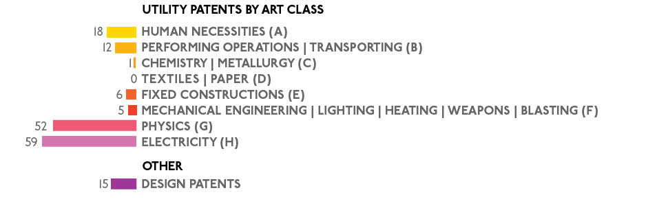
TOP LOCAL ASSIGNEES (NO. OF PATENTS)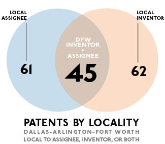
SanDisk Technologies LLC (Addison) 21
Texas Instruments Incorporated (Dallas) 19
Bell Helicopter Textron Inc. (Fort Worth) 8
Futurewei Technologies, Inc. (Plano) 6
Toyota Motor Engineering Manufacturing North America, Inc. (Plano) 4
Frito-Lay North America, Inc. (Plano) 3
UNASSIGNED 11
TOP LOCAL INVENTOR (NO. OF PATENTS)
David Gerard Ledet (Allen) 2
Jonathan Scott Wood (Plano) 2
Kent Poteet (Lucas) 2
FIRST SEEN
(COMPANIES THAT MAY BE ORIGINATING A PATENT IN DFW FOR THE FIRST TIME IN 2019, ACCORDING TO PATENT INDEX.)
Haag Engineering
Patent No. 10380316
System and method for visualization of a mechanical integrity program
Med Hab.
Patent No. 10380866
Dual case system for fall detection device
Precision-Hayes International
Patent No. 10378210
Concrete tendon gripping and sealing apparatus and method
Safe-Fire Technology
Patent No. 10378957
System and method for measuring coal burner flame temperature profile using optical device
Traxxas LP
Patent No. D0856434
Front side molding for a model vehicle
SPEED: APPLICATION TO ISSUE (NO. OF DAYS)
![]() 194 days
194 days
Short-range cross-device authorization
Patent No. 10382960-B1
Assignee: United Services Automobile Association (USAA) (San Antonio)
Inventor: Adrian Borunda (Celina), Cale Riley Spratt (Plano), Jeffrey Joseph Szcinski (Carrollton), Richard Tanner (McKinney)
![]() 2,804 days
2,804 days
Multi-staged water manifold system for a water source heat pump
Patent No. 10378800-B2
Assignee: Lennox Industries Inc. (Richardson)
Inventor: AdrAylan Him (Coppell), Eric Perez (Hickory Creek), Miguel Montemayor (Carrollton), Steve Schneider (Plano)
Don’t miss Dallas Invents: Sign up for the Dallas Innovates e-newsletter.
Patent information is provided by Joe Chiarella, founder of patent analytics company Patent Index and publisher of The Inventiveness Index.
For additional details on the patents granted below, search the USPTO Patent Full-Text and Image Database.
UTILITY PATENTS
H U M A N N E C E S S I T I E S
Dallisgrassweeder a weed surgeon
Patent No. 10375871
Inventor(s): Addis Paul Elmore (Carrollton, TX)
Assignee(s): UNASSIGNED
Law Firm: No Counsel
Application No., Date, Speed: 15979780 on 05/15/2018 (455 days app to issue)
Abstract: A powerful very strong commercial grade hand operated tool for removing weeds intact from a standing position. The tool includes cushions on the handles that are firm and pleasant to use and are replaceable. There are bolts contained in the retaining device that are also replaceable. A completely serviceable tool. There is an ejector disc contained within the retaining device on the bottom end used to expel the weed debris from the tool into a refuse container, this action is spring loaded from the top end of the tool.
[A01B] SOIL WORKING IN AGRICULTURE OR FORESTRY; PARTS, DETAILS, OR ACCESSORIES OF AGRICULTURAL MACHINES OR IMPLEMENTS, IN GENERAL (making or covering furrows or holes for sowing, planting or manuring A01C 5/00; machines for harvesting root crops A01D; mowers convertible to soil working apparatus or capable of soil working A01D 42/04; mowers combined with soil working implements A01D 43/12; soil working for engineering purposes E01, E02, E21)
Method for making a shaped snack chip
Patent No. 10375968
Inventor(s): Richard James Ruegg (Coppell, TX), Rogers Williams (McKinney, TX), Scott Alan Richey (Plano, TX), Sidharth Sambashivan (Dallas, TX), Timothy Allen Johnson (Plano, TX)
Assignee(s): Frito-Lay North America, Inc. (Plano, TX)
Law Firm: Carstens Cahoon, LLP (Local)
Application No., Date, Speed: 14207196 on 03/12/2014 (1980 days app to issue)
Abstract: The invention is an improved process and system for producing a shaped snack chip. A shaping oven, which uses a chain edge conveyor having transverse slats with at least one spring affixed to the slats, is used to convert dough pieces into shaped pre-forms, which can optionally be further dehydrated to form shaped snack chips.
[A47J] KITCHEN EQUIPMENT; COFFEE MILLS; SPICE MILLS; APPARATUS FOR MAKING BEVERAGES [6]
Apparatus and method for rolling sausage rolls
Patent No. 10375970
Inventor(s): Young S Choi (Carrollton, TX)
Assignee(s): UNASSIGNED
Law Firm: No Counsel
Application No., Date, Speed: 15362353 on 11/28/2016 (988 days app to issue)
Abstract: A sausage rolling machine utilizes gravity to reduce costs when rolling a food dough casing around a sausage. A first conveyor rotates in a first direction so as to move a food dough casing toward an edge of the first conveyor. A second conveyor is disposed below the first conveyor. A sausage dispenser dispenses a sausage. A hinged unit is disposed below the sausage dispenser and includes a hinge and a tray portion extending from the hinge. The hinged unit receives the food dough casing that is falling off the edge of the first conveyor when the hinged unit is at rest, initiates wrapping of the food dough casing around the sausage, and rotates the tray portion about the hinge, causing the sausage to roll onto the second conveyor while also causing the sausage to be partially wrapped by the food dough casing.
[A22C] PROCESSING MEAT, POULTRY, OR FISH (preserving A23B; obtaining protein compositions for foodstuffs A23J 1/00; fish, meat or poultry preparations A23L; disintegrating, e.g. chopping meat, B02C 18/00; preparation of proteins C07K 1/00)
Flavor-enhanced beverage product and method of enhancing the flavor thereof
Patent No. 10375976
Inventor(s): Peta-Gaye Chambers (Hawthorne, NY), Rajesh Venkata Potineni (Union, NJ), Stefan K. Baier (Hartsdale, NY), Winsome Johnson (Ossining, NY)
Assignee(s): Frito-Lay North America, Inc. (Plano, TX)
Law Firm: Sterne, Kessler, Goldstein Fox P.L.L.C. (2 non-local offices)
Application No., Date, Speed: 15088575 on 04/01/2016 (1229 days app to issue)
Abstract: A flavor-enhanced beverage includes an added amount of pyroglutamic acid or a salt thereof. The pyroglutamic acid may be in the form of L-pyroglutamic acid, D-pyroglutamic acid, monosodium L-pyroglutamate, monosodium D-pyroglutamate, or a mixture thereof. Both ready-to-drink beverages (such as fruit juices, vegetable juices, coffee, tea, carbonated soft drinks, energy drinks, sports drinks, dairy, and low calorie drinks) as well as concentrated beverages used for the preparation of ready-to-drink beverages benefit from the addition of the pyroglutamic acid. The addition to a beverage product may be in an amount of up to about 3,000 ppm of pyroglutamic acid or a salt thereof, in concentrates, or up to about 300 ppm in ready-to-drink beverages. NULL
Gem applicator assembly
Patent No. 10376025
Inventor(s): Bradley Abbott (Crowley, TX)
Assignee(s): GEMC2, LLC (Wilmington, DE)
Law Firm: Massina Pat TM Law PLLC (1 non-local offices)
Application No., Date, Speed: 16028628 on 07/06/2018 (403 days app to issue)
Abstract: A gem applicator assembly including a dispenser supporting a plurality of gems and an applicator. Each gem has an adhesive backing. The applicator includes a body with a support assembly supported by the body and configured to receive and support the dispenser with one of the gems alignable with an application target area. A plunger is supported relative to the body and movable relative thereto between an initial position and an application position wherein the push rod engages the aligned gem and pushes the gem such that the adhesive backing of an aligned gem moves toward the application target area. The gem dispenser may include a disk configuration with a plurality of spaced apart gem openings extending through the disk. Each gem is aligned with a respective gem opening.
[A44C] JEWELLERY; BRACELETS; OTHER PERSONAL ADORNMENTS; COINS
Umbrella opening and closing system
Patent No. 10376027
Inventor(s): Gregory G. Kuelbs (Westlake, TX)
Assignee(s): Lakesouth Holdings, LLC (Southlake, TX)
Law Firm: No Counsel
Application No., Date, Speed: 15659326 on 07/25/2017 (749 days app to issue)
Abstract: An umbrella apparatus having a canopy portion hingedly coupled to a pole portion. The umbrellas apparatus includes a rechargeable electrical power system that provides electrical power to an electromechanical opening and closing system and a light assembly and an entertainment system. A solar energy system is conductively coupled to the rechargeable electrical power system and is utilized to collect and convert solar energy to electrical energy for recharging the electrical power system. The entertainment system features a USB port and allows users to stream music and control the color of the light assembly.
[A45B] WALKING STICKS (walking aids, e.g. sticks, for blind persons A61H 3/06); UMBRELLAS; LADIES’ OR LIKE FANS (cane or umbrella stands or holders A47G 25/12)
Wall-mounted workstation sliding guide assembly
Patent No. 10376042
Inventor(s): Michael John Sears (Dallas, TX), Simon Nicholas Johnson (Rowlett, TX)
Assignee(s): UNASSIGNED
Law Firm: Law Office of Sam Sokhansanj PLLC (Local + 690 other metros)
Application No., Date, Speed: 15395394 on 12/30/2016 (956 days app to issue)
Abstract: A wall-mounted workstation support assembly that allows users of various heights to quickly, safely, and easily vertically adjust the height of one or more peripherals, monitors, keyboards, and various computing devices. In one aspect, the workstation support assembly includes an elongated track, a first mount having a first guide, wherein the first guide is configured to slide along the elongated track, and a lift and release member. Here, the lift and release member can further include a handle, a first bracket, and a friction member secured to the bracket, wherein the friction member is configured to engage the elongated track and prevent the first mount from sliding along the track.
[A47B] TABLES; DESKS; OFFICE FURNITURE; CABINETS; DRAWERS; GENERAL DETAILS OF FURNITURE (jointing of furniture F16B 12/00)
Athletic facility furniture
Patent No. 10376049
Inventor(s): Sam Allen (Maypearl, TX)
Assignee(s): UNASSIGNED
Law Firm: No Counsel
Application No., Date, Speed: 15878578 on 01/24/2018 (566 days app to issue)
Abstract: A locker includes a pair of spaced-apart upstanding sidewalls, at least one member extending between the sidewalls, the member having a pair of ends, a tongue formed on each end of the member, a groove formed in each sidewall, each groove dimensioned to receive the tongue formed in the end of the member; and a metallic reinforcing member secured to each of the member and the sidewall at an intersection thereof.
[A47B] TABLES; DESKS; OFFICE FURNITURE; CABINETS; DRAWERS; GENERAL DETAILS OF FURNITURE (jointing of furniture F16B 12/00)
Leaning chair
Patent No. 10376071
Inventor(s): David Patton (Flower Mound, TX), Lio Yenwei Chang (Lewisville, TX)
Assignee(s): Variadesk, LLC (Coppell, TX)
Law Firm: Venable LLP (7 non-local offices)
Application No., Date, Speed: 15362324 on 11/28/2016 (988 days app to issue)
Abstract: A leaning chair can include a base defining a lower surface that rests on a floor, the base including a support surface; a shaft coupled to the base, the shaft defining a first end and a second end; a flexible mount coupling the first end of the shaft to the base, the shaft extending through the mount; a pivot pin located underneath the mount, the first end of the shaft resting on the pivot pin, and being configured to be housed inside the mount, the pivot pin being configured to pivot on the support surface; and a user support member coupled to the second end of the shaft.
[A47C] CHAIRS (seats specially adapted for vehicles B60N 2/00); SOFAS; BEDS (upholstery in general B68G)
Warewasher machine drying system and method
Patent No. 10376130
Inventor(s): Joseph F. Sanders (North Richland Hills, TX)
Assignee(s): ILLINOIS TOOL WORKS INC. (Glenview, IL)
Law Firm: Thompson Hine LLP (6 non-local offices)
Application No., Date, Speed: 15298403 on 10/20/2016 (1027 days app to issue)
Abstract: A warewash machine for washing wares includes a chamber for receiving wares, the chamber having at least one wash zone with an associated spray system for spraying liquid onto wares passing therethrough, wherein a downstream drying zone includes a blower for blowing air onto wares passing therethrough. The blower includes an ambient intake operatively connected to an ambient air flow path, a machine intake operatively connected to an internal machine air flow path and an exhaust intake operatively connected to a machine exhaust air flow path.
[A47L] DOMESTIC WASHING OR CLEANING (brushes A46B; cleaning quantities of bottles or of other hollow articles of one kind B08B 9/00; laundry D06F); SUCTION CLEANERS IN GENERAL (cleaning in general B08)
Method and apparatus for low complexity ultrasound based heart rate detection
Patent No. 10376243
Inventor(s): Jonathon David Spaulding (Mountain View, CA), Sourabh Ravindran (Dallas, TX)
Assignee(s): Texas Instruments Incorporated (Dallas, TX)
Law Firm: No Counsel
Application No., Date, Speed: 14497295 on 09/25/2014 (1783 days app to issue)
Abstract: A method for ultrasound based heart rate detection in a heart rate monitoring system is provided that includes receiving a demodulated Doppler ultrasound signal, applying a bandpass filter to the demodulated Doppler ultrasound signal to remove a direct current (DC) component and out-of-band noise, wherein a filtered demodulated Doppler ultrasound signal is generated, rectifying the filtered demodulated Doppler ultrasound signal to generate a rectified filtered demodulated Doppler ultrasound signal, applying a low-pass filter to the rectified filtered demodulated Doppler ultrasound signal to filter out undesired components to leave a resulting signal corresponding to power shift due to heart rate, detecting peaks in the resulting signal, and computing a heart rate based on the detected peaks.
[A61B] DIAGNOSIS; SURGERY; IDENTIFICATION (analysing biological material G01N, e.g. G01N 33/48)
Bone plate and plating system for use of same
Patent No. 10376290
Inventor(s): Steve Courtney (Plano, TX)
Assignee(s): Eminent Spine LLC (Georgetown, TX)
Law Firm: Griggs Bergen LLP (Local)
Application No., Date, Speed: 14242670 on 04/01/2014 (1960 days app to issue)
Abstract: A bone plate and plating system are for use of the same are disclosed. The bone plate includes a body having a span sufficient to overlap a portion of a bone. A screw hole extends through the body in order to receive a bone screw to attach for engaging the plate to the bone. The screw hole includes a counterbore having a beveled surface that intersects at a pinch point a bore having a conical surface of revolution that transitions into the bone engaging surface of the body. The beveled surface includes a variable geometry defining interleaved and rotationally-spaced contact and non-contact bone screw regions.
[A61B] DIAGNOSIS; SURGERY; IDENTIFICATION (analysing biological material G01N, e.g. G01N 33/48)
Method of inserting a vein filter
Patent No. 10376353
Inventor(s): David M. Schaller (Wallingford, PA), James Erich Bressler (Langhorne, PA), James F. McGuckin, Jr. (Radnor, PA)
Assignee(s): Argon Medical Devices Inc. (Plano, TX)
Law Firm: IpHorgan Ltd. (1 non-local offices)
Application No., Date, Speed: 15461258 on 03/16/2017 (880 days app to issue)
Abstract: A method of implanting a vessel filter by a femoral approach comprising the steps of providing a delivery sheath with a substantially straight distal tip and inserting a curved device into the sheath to move the sheath to a second configuration. In the second position, the distal tip of the sheath is curved at an angle to a longitudinal axis of the sheath. The method further comprises the step of rotating the sheath and pusher so a distal opening of the sheath has a more centered position within the vessel.
[A61F] FILTERS IMPLANTABLE INTO BLOOD VESSELS; PROSTHESES; DEVICES PROVIDING PATENCY TO, OR PREVENTING COLLAPSING OF, TUBULAR STRUCTURES OF THE BODY, E.G. STENTS; ORTHOPAEDIC, NURSING OR CONTRACEPTIVE DEVICES; FOMENTATION; TREATMENT OR PROTECTION OF EYES OR EARS; BANDAGES, DRESSINGS OR ABSORBENT PADS; FIRST-AID KITS (dental prosthetics A61C) [2006.01]
Oral appliance
Patent No. 10376408
Inventor(s): Alastair Edwin McAuley (Auckland, , NZ), W. Keith Thornton (Dallas, TX)
Assignee(s): Airway Technologies, LLC (Carrollton, TX)
Law Firm: Baker Botts L.L.P. (Local + 8 other metros)
Application No., Date, Speed: 14931942 on 11/04/2015 (1378 days app to issue)
Abstract: An oral appliance includes an upper arch, a lower arch, and an electronic device. The upper arch is configured to be positioned within a user”s mouth proximate the user”s maxillary dentition when the upper arch is positioned in the user”s mouth. The lower arch is configured to be positioned proximate the user”s mandibular dentition when the lower arch is positioned in the user”s mouth. The electronic device is coupled to one or more of the upper arch and the lower arch, the electronic device configured to monitor a feature of the environment proximate one or more of the upper arch and the lower arch.
[A61F] FILTERS IMPLANTABLE INTO BLOOD VESSELS; PROSTHESES; DEVICES PROVIDING PATENCY TO, OR PREVENTING COLLAPSING OF, TUBULAR STRUCTURES OF THE BODY, E.G. STENTS; ORTHOPAEDIC, NURSING OR CONTRACEPTIVE DEVICES; FOMENTATION; TREATMENT OR PROTECTION OF EYES OR EARS; BANDAGES, DRESSINGS OR ABSORBENT PADS; FIRST-AID KITS (dental prosthetics A61C) [2006.01]
Uni-port hybrid gauge surgical apparatuses and methods
Patent No. 10376414
Inventor(s): Walter J. Stark, III (Fort Worth, TX)
Assignee(s): Novartis AG (Basel, , CH)
Law Firm: No Counsel
Application No., Date, Speed: 15376857 on 12/13/2016 (973 days app to issue)
Abstract: Systems, apparatuses, and methods include a surgical apparatus with a handle for grasping by a user and a multi-function surgical portion extending therefrom. The multi-function surgical portion may include an illuminator portion arranged to provide illumination to a surgical region of a patient during a surgical procedure, and tissue-treating portion coaxially aligned with the illuminator portion.
[A61F] FILTERS IMPLANTABLE INTO BLOOD VESSELS; PROSTHESES; DEVICES PROVIDING PATENCY TO, OR PREVENTING COLLAPSING OF, TUBULAR STRUCTURES OF THE BODY, E.G. STENTS; ORTHOPAEDIC, NURSING OR CONTRACEPTIVE DEVICES; FOMENTATION; TREATMENT OR PROTECTION OF EYES OR EARS; BANDAGES, DRESSINGS OR ABSORBENT PADS; FIRST-AID KITS (dental prosthetics A61C) [2006.01]
Method of treating or preventing tumors of the central nervous system
Patent No. 10376477
Inventor(s): John Patrick McCook (Frisco, TX)
Assignee(s): Berg LLC (Framingham, MA)
Law Firm: McCarter English, LLP (7 non-local offices)
Application No., Date, Speed: 15376243 on 12/12/2016 (974 days app to issue)
Abstract: The invention provides methods and compositions for treatment of a subject with a central nervous system (CNS) tumor comprising administration of Coenzyme Q10 (CoQ10), particularly when the subject exhibits at least one CNS abnormality as a result of the tumor.
[A61K] PREPARATIONS FOR MEDICAL, DENTAL, OR TOILET PURPOSES (devices or methods specially adapted for bringing pharmaceutical products into particular physical or administering forms A61J 3/00; chemical aspects of, or use of materials for deodorisation of air, for disinfection or sterilisation, or for bandages, dressings, absorbent pads or surgical articles A61L; soap compositions C11D)
Touch screen safety controls for clinician programmer
Patent No. 10376701
Inventor(s): Norbert Kaula (Arvada, CO), Yohannes Iyassu (Denver, CO)
Assignee(s): NUVECTRA CORPORATION (Plano, TX)
Law Firm: Haynes and Boone, LLP (Local + 13 other metros)
Application No., Date, Speed: 15191606 on 06/24/2016 (1145 days app to issue)
Abstract: One or more virtual objects are displayed on an electronic programmer. The virtual objects represent initiating and terminating a delivery of a medical therapy to a patient. An actuation of the one or more virtual objects is sensed. The delivery of the medical therapy is terminated immediately if the actuation of the one or more virtual objects corresponds to terminating the delivery of the medical therapy. The delivery of the medical therapy is initiated in a delayed manner if the actuation of the one or more virtual objects corresponds to starting the delivery of the medical therapy. A battery level of the electronic programmer is monitored. At least one of the following tasks is performed if the battery level is lower than a target battery level: disallowing programming of the electronic programmer; terminating the delivery of an existing medical therapy; and precluding the delivery of a prospective medical therapy.
[A61N] ELECTROTHERAPY; MAGNETOTHERAPY; RADIATION THERAPY; ULTRASOUND THERAPY (measurement of bioelectric currents A61B; surgical instruments, devices or methods for transferring non-mechanical forms of energy to or from the body A61B 18/00; anaesthetic apparatus in general A61M; incandescent lamps H01K; infra-red radiators for heating H05B) [6]
System and method for the validation and quality assurance of computerized contours of human anatomy
Patent No. 10376715
Inventor(s): Jun Tan (Coppell, TX)
Assignee(s): Washington University (St. Louis, MO)
Law Firm: Armstrong Teasdale LLP (7 non-local offices)
Application No., Date, Speed: 14700592 on 04/30/2015 (1566 days app to issue)
Abstract: A system and method for validating the accuracy of delineated contours in computerized imaging using statistical data for generating assessment criterion that define acceptable tolerances for delineated contours, with the statistical data being conditionally updated and/or refined between individual processes for validating delineated contours to thereby adjust the tolerances defined by the assessment criterion in the stored statistical data, such that the stored statistical data is more closely representative of a target population. In an alternative embodiment, a system and method for validating the accuracy of delineated contours in computerized imaging using machine learning for assessing delineated contours, with the machine learning training data being used to generate geometric attributes, and the geometric attributes used to construct intra- and interstructural geometric attribute distribution models to automatically detect contouring errors. The present invention may be used to facilitate, as one example, radiation therapy.
[A61N] ELECTROTHERAPY; MAGNETOTHERAPY; RADIATION THERAPY; ULTRASOUND THERAPY (measurement of bioelectric currents A61B; surgical instruments, devices or methods for transferring non-mechanical forms of energy to or from the body A61B 18/00; anaesthetic apparatus in general A61M; incandescent lamps H01K; infra-red radiators for heating H05B) [6]
O P E R A T I O N S & T R A N S P O R T
Secure medication delivery
Patent No. 10376444
Inventor(s): Ira L. Allen (Dallas, TX)
Assignee(s): International Business Machines Corporation (Armonk, NY)
Law Firm: No Counsel
Application No., Date, Speed: 15076941 on 03/22/2016 (1239 days app to issue)
Abstract: A method includes micro-machining a cavity within a substrate, filling the cavity with a medication, forming a sealing layer over the cavity, micro-machining a cantilevered beam from a layer of material, the cantilevered beam comprising a tip for puncturing the sealing layer, and attaching the cantilevered beam to the substrate such that moving the cantilevered beam toward the substrate enables the tip to puncture the sealing layer. A computer program product corresponding to the method is also disclosed. An apparatus includes a substrate having a cavity micro-machined therein, a sealing layer formed over the cavity, a medication disposed within the cavity, a cantilevered beam micro-machined from a layer of material, the cantilevered beam comprising a tip for puncturing the sealing layer, and the cantilevered beam attached to the substrate and disposed to enable the tip to puncture the sealing layer when the cantilevered beam is moved towards the substrate.
[B65D] CONTAINERS FOR STORAGE OR TRANSPORT OF ARTICLES OR MATERIALS, e.g. BAGS, BARRELS, BOTTLES, BOXES, CANS, CARTONS, CRATES, DRUMS, JARS, TANKS, HOPPERS, FORWARDING CONTAINERS; ACCESSORIES, CLOSURES, OR FITTINGS THEREFOR; PACKAGING ELEMENTS; PACKAGES
Separation apparatus with screen having fixed, non-uniform openings
Patent No. 10376924
Inventor(s): Joseph H. Gold (Dallas, TX), Kevin C. Cogan (Oak Point, TX)
Assignee(s): Frito-Lay North America, Inc. (Plano, TX)
Law Firm: Carstens Cahoon, LLP (Local)
Application No., Date, Speed: 15440267 on 02/23/2017 (901 days app to issue)
Abstract: A novel separation screen, a separation apparatus utilizing the separation screen, and a method for product separation are disclosed herein. The separation apparatus includes a housing defining a separation chamber having an inlet and a plurality of outlet orifices. A separation screen, which is located within the separation chamber, has a plurality of openings having fixed, non-uniform sizes. The separation apparatus also includes an adjustable feed placement device located upstream from the separation screen to direct a feed stream to a selected region of the separation screen to achieve a desired size distribution in each of the product streams.
[B07B] SEPARATING SOLIDS FROM SOLIDS BY SIEVING, SCREENING, OR SIFTING OR BY USING GAS CURRENTS; OTHER SEPARATING BY DRY METHODS APPLICABLE TO BULK MATERIAL, e.g. LOOSE ARTICLES FIT TO BE HANDLED LIKE BULK MATERIAL (wet separating processes, sorting by processes using fluent material in the same way as liquid B03; combinations of dry separating apparatus with wet separating apparatus B03B; using liquids B03B, B03D; sorting by magnetic or electrostatic separation of solid materials from solid materials or fluids, separation by high voltage electric fields B03C; centrifuges or vortex apparatus for carrying out physical processes B04; hand sorting, postal sorting, sorting by switching or other devices actuated in response to detection or measurement of some feature of articles or samples of material B07C)
Glueless pocketed spring unit construction
Patent No. 10376983
Inventor(s): Martin Wolfson (Dallas, TX)
Assignee(s): UNASSIGNED
Law Firm: Carrington, Coleman, Sloman Blumenthal, L.L.P. (Local)
Application No., Date, Speed: 15185774 on 06/17/2016 (1152 days app to issue)
Abstract: Methods and systems for no-glue pocketed spring unit construction. Rows of pocketed springs, preferably arranged into modules of more than two pocketed springs surrounding a central hole, are ultrasonically welded together when paired vibrating probes and anvils press layers of pocketed spring fabric from the rows of pocketed springs together and a welding pulse is transmitted to the vibrating probe.
[B23K] SOLDERING OR UNSOLDERING; WELDING; CLADDING OR PLATING BY SOLDERING OR WELDING; CUTTING BY APPLYING HEAT LOCALLY, e.g. FLAME CUTTING; WORKING BY LASER BEAM (making metal-coated products by extruding metal B21C 23/22; building up linings or coverings by casting B22D 19/08; casting by dipping B22D 23/04; manufacture of composite layers by sintering metal powder B22F 7/00; arrangements on machine tools for copying or controlling B23Q; covering metals or covering materials with metals, not otherwise provided for C23C; burners F23D)
Alternative-fuel gas orifice having principal-fuel gas orifice temperature profile and a heating, ventilation and air conditioning system incorporating the same
Patent No. 10376999
Inventor(s): Glenn W. Kowald (Carrollton, TX), Hans J. Paller (Double Oak, TX)
Assignee(s): Lennox Industries Inc. (Richardson, TX)
Law Firm: Winstead PC (Local + 2 other metros)
Application No., Date, Speed: 15368882 on 12/05/2016 (981 days app to issue)
Abstract: An alternative-fuel gas orifice, a gas furnace configured to employ the same and a method of designing a gas orifice. In one embodiment, the gas orifice includes: (1) a body having an aperture extending therethrough and including: (1a) a metering neck having a cross-sectional area such that a given flow rate of a gas is established when the gas is delivered to the gas orifice at a given alternative-fuel delivery pressure and (1b) a diffuser having a cross-sectional area larger than the cross-sectional area of the metering neck and a length such that the gas achieves a substantially laminar flow before exiting the diffuser.
[B23P] OTHER WORKING OF METAL; COMBINED OPERATIONS; UNIVERSAL MACHINE TOOLS (arrangements for copying or controlling B23Q)
Vehicle proximity condition detection and haptic notification system
Patent No. 10377307
Inventor(s): Danil V. Prokhorov (Canton, MI), Hideki Hada (Ann Arbor, MI)
Assignee(s): Toyota Motor Engineering Manufacturing North America, Inc. (Plano, TX)
Law Firm: Darrow Mustafa PC (2 non-local offices)
Application No., Date, Speed: 15951832 on 04/12/2018 (488 days app to issue)
Abstract: A computing device for a vehicle proximity condition detection and haptic notification system is provided. The device includes one or more processors for controlling operation of the computing device, and a memory for storing data and program instructions usable by the one or more processors. The one or more processors are configured to execute instructions stored in the memory to enable a user to specify operation of an active suspension system of an ego-vehicle so as to generate at least one pulse at at least one wheel of the vehicle, responsive to a vehicle proximity condition, and operate the active suspension system in accordance with the user”s specification.
[B60G] VEHICLE SUSPENSION ARRANGEMENTS (air-cushion vehicles B60V; connections between vehicle bodies and vehicle frames B62D 24/00) [5]
Rotorcraft with redundant processors using state comparison
Patent No. 10377470
Inventor(s): Jillian Samantha Alfred (Ft. Worth, TX)
Assignee(s): Bell Helicopter Textron Inc. (Fort Worth, TX)
Law Firm: Slater Matsil, LLP (Local + 1 other metros)
Application No., Date, Speed: 15646894 on 07/11/2017 (763 days app to issue)
Abstract: A system and method for providing state comparison of redundant processors used, e.g. to control a rotor craft. A primary microprocessor is configured to receive input data from a position sensor and a flight condition sensor and determine therefrom a first desired control law state, and a secondary microprocessor is configured to receive input data from the position sensor and the flight condition sensor and determine therefrom a second desired control law state. The first desired control law state from the primary microprocessor and the second desired control law state from the secondary microprocessor are compared, and (a) the first desired control law state is entered when the first desired control law state and the second desired control law state match, and (b) a last known control law state is maintained when the first desired control law state and the second desired control law state do not match.
[B64C] AEROPLANES; HELICOPTERS (air-cushion vehicles B60V)
Disconnecting a rotor
Patent No. 10377473
Inventor(s): Carlos A. Fenny (Arlington, TX), Charles J. Kilmain (Fort Worth, TX), David Sembritzky (Grapevine, TX), Gary A. Cope (Keller, TX), Ryan T. Ehinger (Irving, TX)
Assignee(s): Bell Helicopter Textron Inc. (Fort Worth, TX)
Law Firm: No Counsel
Application No., Date, Speed: 13733952 on 01/04/2013 (2412 days app to issue)
Abstract: According to one embodiment, a clutch may be coupled between a rotor system and a power train of a rotorcraft. The clutch may be operable to disengage the rotor system from the power train during operation of the power train. A clutch control system in communication with the clutch and include a rotorcraft condition sensor operable to sense an operating condition of the rotorcraft and a control unit operable to prevent the clutch from disengaging the rotor system from the power train if the operating condition of the rotorcraft fails to satisfy a predetermined criterion.
[B64C] AEROPLANES; HELICOPTERS (air-cushion vehicles B60V)
Adjustable pitch link
Patent No. 10377477
Inventor(s): Clifton B. Day (Weatherford, TX), Daniel Spivey (Fort Worth, TX), Frank B. Stamps (Colleyville, TX), Joseph Biser (Euless, TX)
Assignee(s): BELL HELICOPTER TEXTRON INC. (Fort Worth, TX)
Law Firm: Lightfoot Alford PLLC (1 non-local offices)
Application No., Date, Speed: 13669212 on 11/05/2012 (2472 days app to issue)
Abstract: According to one embodiment, a pitch link includes a first link, a second link coupled to a first end of the first link, a third link coupled to a second end of the first link opposite the first end, and a first bearing housing having a first bearing and a second bearing housing having a second bearing. The first bearing housing is removably coupled to the second link. The second link separates the first bearing housing from the first link. The second bearing housing is removably coupled to the third link. The third link separates the second bearing housing from the first link.
[B64C] AEROPLANES; HELICOPTERS (air-cushion vehicles B60V)
Variable directional thrust for helicopter tail anti-torque system
Patent No. 10377479
Inventor(s): Carlos Alexander Fenny (Fort Worth, TX), Erik John Oltheten (Fort Worth, TX), Thomas Dewey Parsons (Fort Worth, TX)
Assignee(s): BELL HELICOPTER TEXTRON INC. (Fort Worth, TX)
Law Firm: Chalker Flores, LLP (Local)
Application No., Date, Speed: 15172811 on 06/03/2016 (1166 days app to issue)
Abstract: The present invention includes an anti-torque assembly for a helicopter comprising a plurality of fixed blade pitch motors mounted on one or more pivots on the tail boom of the helicopter, wherein the plurality of fixed blade pitch motors on the one or more pivots are adapted to be oriented substantially in-plane with a tail boom of a helicopter during a first mode of operation that comprises a hover mode and wherein the fixed blade pitch motors are adapted to be oriented substantially off-plane from the tail boom of the helicopter during a second mode of helicopter operation that is different from the first mode.
[B64C] AEROPLANES; HELICOPTERS (air-cushion vehicles B60V)
Apparatus and method for directing thrust from tilting cross-flow fan wings on an aircraft
Patent No. 10377480
Inventor(s): Daniel B. Robertson (Southlake, TX), Kirk L. Groninga (Keller, TX), Matthew E. Louis (Fort Worth, TX)
Assignee(s): Bell Helicopter Textron Inc. (Fort Worth, TX)
Law Firm: Timmer Law Group, PLLC (1 non-local offices)
Application No., Date, Speed: 15483602 on 04/10/2017 (855 days app to issue)
Abstract: A variable thrust cross-flow fan system for an aircraft including a rotatable wing member having a first housing member; an actuator assembly operably coupled to the first housing member; and a variable thrust cross-flow fan assembly including a first and second driver plates having a plurality of blades rotatably mounted therebetween. The plurality of blades has a circular path of travel when rotating and includes a control assembly coupled to the plurality of blades to generate a variable thrust force. The control assembly includes a control cam that is substantially non-rotatable relative to the first and second driver plates and a hinge member that is fixedly connected to the control cam and to the first housing member at a hinge axis. Rotation of the first housing member by the actuator assembly imparts rotation of the control cam about the hinge axis, thereby changing the direction of the variable thrust force.
[B64C] AEROPLANES; HELICOPTERS (air-cushion vehicles B60V)
Beam springs for aircraft engine mount assemblies
Patent No. 10377502
Inventor(s): Bruce Bennett Bacon (Fort Worth, TX), John Elton Brunken, Jr. (Fort Worth, TX), Michael Edwin Rinehart (Fort Worth, TX), Nick Pravanh (Fort Worth, TX)
Assignee(s): Bell Helicopter Textron Inc. (Fort Worth, TX)
Law Firm: Lawrence Youst PLLC (Local)
Application No., Date, Speed: 15410015 on 01/19/2017 (936 days app to issue)
Abstract: An engine mount assembly for coupling an engine to an airframe. The engine mount assembly includes a torsion bar coupled to the engine and a lateral movement control assembly coupled between the torsion bar and the airframe. The lateral movement control assembly includes a spring having a lateral stiffness. The torsion bar rotates in response to lateral movement of the engine such that the lateral movement of the engine is controllable based on the lateral stiffness of the spring.
[B64D] EQUIPMENT FOR FITTING IN OR TO AIRCRAFT; FLYING SUITS; PARACHUTES; ARRANGEMENTS OR MOUNTING OF POWER PLANTS OR PROPULSION TRANSMISSIONS IN AIRCRAFT
Simplified power conversion systems for vehicles
Patent No. 10381967
Inventor(s): Jae Seung Lee (Ann Arbor, MI), Jongwon Shin (Ann Arbor, MI)
Assignee(s): TOYOTA MOTOR ENGINEERING MANUFACTURING NORTH AMERICA, INC. (Plano, TX)
Law Firm: Dinsmore Shohl LLP (14 non-local offices)
Application No., Date, Speed: 15597810 on 05/17/2017 (818 days app to issue)
Abstract: A power conversion system for a vehicle includes a power conditioning device, a boost converter, an inverter coupled to the boost converter, a transformer, a second rectifier coupled to the transformer, an electric motor, a battery coupled to the second rectifier, a first switch configured to selectively connect the boost converter with the power conditioning device or the battery, and a second switch configured to selectively connect the inverter with the transformer or the electric motor. The first switch connects the power conditioning device with the boost converter and the second switch connects the inverter with the transformer in response to the vehicle being in a grid-connected mode, and the first switch connects the battery with the boost converter and the second switch connects the inverter with the electric motor in response to the vehicle being in a stand-alone mode.
[B60R] VEHICLES, VEHICLE FITTINGS, OR VEHICLE PARTS, NOT OTHERWISE PROVIDED FOR (fire prevention, containment or extinguishing specially adapted for vehicles A62C 3/07)
C H E M I S T R Y & M E T A L L U R G Y
Cultivation bag for cultivating microbes
Patent No. 10377982
Inventor(s): Wei K. Hsu (Plano, TX)
Assignee(s): UNASSIGNED
Law Firm: Griggs Bergen LLP (Local)
Application No., Date, Speed: 16238410 on 01/02/2019 (223 days app to issue)
Abstract: A cultivation bag assembly for the cultivation of microbes, fungi and other organisms includes a bag having first and second walls joined along side edges to define a bag interior for containing a food substrate and an organism to be cultivated. At least one of the first and second walls is constructed of a layer of water-vapor permeable material to allow the passage of water vapor therethrough. A bag wall overlay layer formed from gas impermeable layer is releasably coupled to the bag. The overlay layer overlays the layer of water-vapor permeable material to prevent the passage of gases therethrough. The bag wall overlay layer has an opening with a gas filter patch covering the opening to allow the passage of oxygen and carbon dioxide gases through the gas filter patch to and from ambient air to facilitate incubation of the organism within the interior of the bag. The bag wall overlay layer is removable from the bag to allow water vapor to pass through the layer of water-vapor permeable material to ambient air facilitate drying of the bag contents after incubation is complete.
[C12M] APPARATUS FOR ENZYMOLOGY OR MICROBIOLOGY (installations for fermenting manure A01C 3/02; preservation of living parts of humans or animals A01N 1/02; brewing apparatus C12C; fermentation apparatus for wine C12G; apparatus for preparing vinegar C12J 1/10) [3]
F I X E D C O N S T R U C T I O N S
Method and apparatus for improved installation of caissons
Patent No. 10378171
Inventor(s): Hock Lim (Fort Worth, TX)
Assignee(s): American Transmission Company LLC (Waukesha, WI)
Law Firm: Boyle Fredrickson, S.C. (1 non-local offices)
Application No., Date, Speed: 15603912 on 05/24/2017 (811 days app to issue)
Abstract: A caisson is modified to include side tabs thin can be gripped by side-mounted clamps on a vibratory hammer so that the caisson may be lifted into position from a horizontal position, oriented vertically, and driven into the ground without readjustment of the clamping of the vibratory hammer. An end cap installed permanently at the top of the caisson may provide an additional flange for receiving a lower clamp of the vibratory hammer to complete installation of the caisson, driving the caisson further into the earth until the tabs are buried in the ground. The flange may be sized to fit within a tower portion attached to the caisson eliminating the need for a replaceable flange system.
[E02D] FOUNDATIONS; EXCAVATIONS; EMBANKMENTS (specially adapted for hydraulic engineering E02B); UNDERGROUND OR UNDERWATER STRUCTURES [6]
Concrete tendon gripping and sealing apparatus and method
Patent No. 10378210
Inventor(s): Norris Hayes (Katy, TX)
Assignee(s): PRECISION-HAYES INTERNATIONAL INC. (Seagoville, TX)
Law Firm: Adolph Locklar (2 non-local offices)
Application No., Date, Speed: 15547985 on 02/02/2016 (1288 days app to issue)
Abstract: Methods and devices for sealing and/or gripping concrete strengthening tendons. Some embodiments provide a method of forming a seal between an encapsulated anchor and a sheath of a tendon engaging the encapsulated anchor. Other embodiments provide a splice for forming a seal around a discontinuity in the sheath of a concrete tensioning tendon. Some embodiments provide a seal assembly for forming a seal between a tubular extension and a sheath of a tendon to protect an exposed portion of the tendon contained within the tubular extension. Some embodiments also provide a method of forming a fluid tight seal between tubular extension and a sheath of a tendon, while other embodiments provide a method of gripping the sheath of a tendon with a tubular extension to prevent the sheath from moving relative to the extension.
[E04C] STRUCTURAL ELEMENTS; BUILDING MATERIALS (for bridges E01D; specially designed for insulation or other protection E04B; elements used as building aids E04G; for mining E21; for tunnels E21D; structural elements with broader range of application than for building engineering F16, particularly F16S)
Storage and deployment system for a composite slickline
Patent No. 10378294
Inventor(s): Dominick Joseph Bellotte (Flower Mound, TX), Richard Mineo (Richardson, TX)
Assignee(s): Halliburton Energy Services, Inc. (Houston, TX)
Law Firm: McGuireWoods LLP (Local + 9 other metros)
Application No., Date, Speed: 15322243 on 07/31/2014 (1839 days app to issue)
Abstract: A slickline for use in a wellbore comprising: the slickline, wherein the slickline: comprises a composite material comprising a plurality of carbon fiber strands, and is housed on the inside of a receptacle, wherein the receptacle is hollow and cone-shaped. The slickline can also be made from an anisotropic material; and wherein a first test section of the slickline has a stiffness greater than a second test section having the same dimensions as the first test section but made of steel. A method of deploying the slickline into a wellbore comprising: positioning a portion of the slickline into a controlled deployment device, wherein the controlled deployment device comprises a housing; and causing at least a portion of the slickline to enter the wellbore, wherein the slickline moves from the receptacle through the housing and into the wellbore during the step of causing.
[E21B] EARTH OR ROCK DRILLING (mining, quarrying E21C; making shafts, driving galleries or tunnels E21D); OBTAINING OIL, GAS, WATER, SOLUBLE OR MELTABLE MATERIALS OR A SLURRY OF MINERALS FROM WELLS [5]
Select fire switch form factor system and method
Patent No. 10378320
Inventor(s): James A. Rollins (Lipan, TX), John T. Hardesty (Fort Worth, TX)
Assignee(s): GEODYNAMICS, INC. (Millsap, TX)
Law Firm: Patent Portfolio Builders PLLC (4 non-local offices)
Application No., Date, Speed: 16025002 on 07/02/2018 (407 days app to issue)
Abstract: A wellbore select fire switch retaining member system and method with an integrated through wire and ground wire in a switch sub. The system/method includes a retaining member that has a form factor acceptable by a conventional switch sub. The retaining member incorporates an electrical connection to the center pin of a pressure switch. The system further includes a secondary piston aligned with a piston in the switch (switch piston) so that external pressure is fully acted upon the entire switch piston creating a reliable switch connection. Another system includes an integrated retaining member and switch module having a form factor compatible with existing switch subs. The integrated module inputs include a ground wire and a through wire and the outputs include a ground wire, through wire and an arming wire.
[E21B] EARTH OR ROCK DRILLING (mining, quarrying E21C; making shafts, driving galleries or tunnels E21D); OBTAINING OIL, GAS, WATER, SOLUBLE OR MELTABLE MATERIALS OR A SLURRY OF MINERALS FROM WELLS [5]
Plastic void construction unit
Patent No. 10378678
Inventor(s): Michael L. Turner (Fort Worth, TX)
Assignee(s): UNASSIGNED
Law Firm: Law Office of Jeff Williams PLLC (Local + 690 other metros)
Application No., Date, Speed: 16186224 on 11/09/2018 (277 days app to issue)
Abstract: A device and method for the creation of a water proof component void form unit to create space between concrete structures and expansive soil for the passage of utility conduit lines is described. The unit includes a plurality of panels interlocked with one or more connectors and supports that pass internally through flutes within the panel members. The void space is formed from a singular panel that is scored along a score line. The score line passes only through an upper surface. The panel member is folded about the lower surface at the score line to form the void space. The panels are located in a trench and configured to define a void space underground for the passage of the utility conduit lines. The unit is configured to resist soil expansive forces so as to protect the placement and integrity of the utility conduit lines.
[E02D] FOUNDATIONS; EXCAVATIONS; EMBANKMENTS (specially adapted for hydraulic engineering E02B); UNDERGROUND OR UNDERWATER STRUCTURES [6]
System for nuclear waste storage and monitoring
Patent No. 10381122
Inventor(s): Marlan Downey (Dallas, TX)
Assignee(s): MWD-IP Holdings, LLC (Dallas, TX)
Law Firm: No Counsel
Application No., Date, Speed: 16103269 on 08/14/2018 (364 days app to issue)
Abstract: A system for storing and monitoring nuclear waste. The system includes a storage borehole having an end segment configured to store nuclear waste in a subterranean storage site location having a shale rock layer. The layer has a measured fluid overpressure in a range corresponding to greater than hydrostatic pressure to less than a lithostatic pressure from overlying rock layers. The system also includes a monitoring borehole configured to reside in the layer with an end segment of the monitoring borehole in a vicinity of the end segment of the storage borehole. The measured fluid pressure at the end of the monitoring borehole is in the fluid overpressure range.
[E21B] EARTH OR ROCK DRILLING (mining, quarrying E21C; making shafts, driving galleries or tunnels E21D); OBTAINING OIL, GAS, WATER, SOLUBLE OR MELTABLE MATERIALS OR A SLURRY OF MINERALS FROM WELLS [5]
M E C H A N I C A L E N G I N E E R I N G
LIGHTING | HEATING | WEAPONS | BLASTING
Cooling systems for vehicle interior surfaces
Patent No. 10377407
Inventor(s): Brian J. Pinkelman (Ann Arbor, MI), Shailesh Joshi (Ann Arbor, MI), Umesh N. Gandhi (Farmington Hills, MI)
Assignee(s): Toyota Motor Engineering Manufacturing North America, Inc. (Plano, TX)
Law Firm: Darrow Mustafa PC (2 non-local offices)
Application No., Date, Speed: 15427259 on 02/08/2017 (916 days app to issue)
Abstract: A vehicle component includes a first volume of phase change material and a second volume of phase change material spaced apart from the first volume of phase change material. The first volume of phase change material contains a greater mass of phase change material than the second volume of phase change material. The component also includes a thermally-conductive structure in direct contact with both the first volume of phase change material and the second volume of phase change material, so as to facilitate heat transfer between the first volume of phase change material and the second volume of phase change material.
[F28D] HEAT-EXCHANGE APPARATUS, NOT PROVIDED FOR IN ANOTHER SUBCLASS, IN WHICH THE HEAT-EXCHANGE MEDIA DO NOT COME INTO DIRECT CONTACT (heat-transfer, heat-exchange or heat-storage materials C09K 5/00; fluid heaters having heat generating means and heat transferring means F24H; furnaces F27; details of heat-exchange apparatus of general application F28F); HEAT STORAGE PLANTS OR APPARATUS IN GENERAL [4]
Valve plug assembly and seat ring for regulator
Patent No. 10378657
Inventor(s): Chun Lin (McKinney, TX)
Assignee(s): EMERSON PROCESS MANAGEMENT REGULATOR TECHNOLOGIES, INC. (McKinney, TX)
Law Firm: Marshall, Gerstein Borun LLP (2 non-local offices)
Application No., Date, Speed: 15469305 on 03/24/2017 (872 days app to issue)
Abstract: A valve plug assembly adapted for sealing engagement with a seat ring. The valve plug assembly includes a valve plug having a sealing disk adapted to engage a seating surface the seat ring. The seating surface of the seat ring has a primary portion with a primary angle of any one of about 20 degrees to about 45 degrees and a secondary portion extending from the primary portion with a secondary angle of about 10 degrees. A retainer is coupled to the valve plug and includes a body having a first portion, a second portion, and a side extending from the first portion to the second portion at one of an angle of about 30 degrees to about 45 degrees. So configured, the stress acting on the sealing surface is reduced, increasing the service life of the sealing disk.
[F16K] VALVES; TAPS; COCKS; ACTUATING-FLOATS; DEVICES FOR VENTING OR AERATING
Light panel retro-fit kits
Patent No. 10378699
Inventor(s): Jordon Musser (Dallas, TX)
Assignee(s): Flex Ltd (Singapore, , SG)
Law Firm: Weber Rosselli Cannon LLP (no location found)
Application No., Date, Speed: 15687045 on 08/25/2017 (718 days app to issue)
Abstract: The present disclosure is directed to a lighting retro-fit assembly including a panel configured for the passage of light therethrough, at least one light emitting diode (LED) secured to the panel, a driver electrically connected to the at least one LED, and an extendible suspension device, where the extendible suspension device permits mechanical connection of the panel to an existing lighting structure while enabling access to the driver.
[F21K] LIGHT SOURCES NOT OTHERWISE PROVIDED FOR
Segmented watertube boiler system
Patent No. 10378755
Inventor(s): Jimmie P. Caradine (Commerce, TX)
Assignee(s): UNASSIGNED
Law Firm: Eldredge Law Firm, LLC (2 non-local offices)
Application No., Date, Speed: 15832034 on 12/05/2017 (616 days app to issue)
Abstract: A segmented watertube boiler system allows for rapidly expanding the capacity of a boiler. The system joins boiler segments to form a boiler. The segments have portions of the boiler so that the storage capacity for water and heat are increased with the number of segments uses. Any openings in the segments on the ends are capped off and heat and water sources are attached. The boiler can be cleaned and maintained by simply disassembling the segments to provide access to the whole boiler.
[F22B] METHODS OF STEAM GENERATION; STEAM BOILERS (steam engine plants where engine aspects predominate F01K; removal of combustion products or residues, e.g. cleaning of the combustion contaminated surfaces of tubes of boilers, F23J 3/00; domestic central-heating systems using steam F24D; heat exchange or heat transfer in general F28; generation of vapour in the cores of nuclear reactors G21)
Multi-staged water manifold system for a water source heat pump
Patent No. 10378800
Inventor(s): Aylan Him (Coppell, TX), Eric Perez (Hickory Creek, TX), Miguel Montemayor (Carrollton, TX), Steve Schneider (Plano, TX)
Assignee(s): Lennox Industries Inc. (Richardson, TX)
Law Firm: Winstead PC (Local + 2 other metros)
Application No., Date, Speed: 13316206 on 12/09/2011 (2804 days app to issue)
Abstract: One aspect, as provided herein, is directed to a multi-stage fluid control system for a fluid source heat pump system. This embodiment comprises compressors configured to operate as separate, heat exchange stages, condensers each being fluidly coupled to at least one of the compressors by refrigerant tubing and having intake ends coupled together by a fluid intake manifold. This embodiment further includes output conduits coupled to each of the condensers and that are couplable to a distal location. Further included is a modulating valve control system interposed the output conduits. The modulating valve control system is configured to stage a flow of fluid through the condensers based on a number of operating compressors.
[F24D] DOMESTIC- OR SPACE-HEATING SYSTEMS, e.g. CENTRAL HEATING SYSTEMS; DOMESTIC HOT-WATER SUPPLY SYSTEMS; ELEMENTS OR COMPONENTS THEREFOR (preventing corrosion C23F; water supply in general E03; using steam or condensate extracted or exhausted from steam engine plants for heating purposes F01K 17/02; steam traps F16T; domestic stoves or ranges F24B, F24C; water or air heaters having heat generating means F24H; combined heating and refrigeration systems F25B; heat exchange apparatus or elements F28; removing furring F28G; electric heating elements or arrangements H05B)
P H Y S I C S
Obtaining breast density measurements and classifications
Patent No. 10376230
Inventor(s): Arunkumar Gururajan (Dallas, TX), James H. Pike (Carrollton, TX), James Monaco (Frisco, TX), Jeffrey C. Wehnes (Richardson, TX), Ronald Larcom (Frisco, TX)
Assignee(s): iCad, Inc. (Nashua, NH)
Law Firm: Loginov Associates, PLLC (1 non-local offices)
Application No., Date, Speed: 15035743 on 11/10/2014 (1737 days app to issue)
Abstract: Breast density measurements are used to perform Breast Imaging Reporting and Data System (BI-RADS) classification during breast cancer screenings. The accuracy of breast density measurements can be improved by quantitatively processing digital mammographic images. For example, breast segmentation may be performed on a mammographic image to isolate the breast tissue from the background and pectoralis tissue, while a breast thickness adjustment may be performed to compensate for decreased tissue thickness near the skin line of the breast. In some instances, BI-RADS density categorization may consider the degree to which dense tissue is dispersed throughout the breast. A breast density dispersion parameter can also be obtained using quantitative techniques, thereby providing objective BI-RADS classifications that are less susceptible to human error.
[G06T] IMAGE DATA PROCESSING OR GENERATION, IN GENERAL [2006.01]
Method and system for passive electroseismic surveying
Patent No. 10378316
Inventor(s): Alan Katz (Dallas, TX), Arthur Thompson (Houston, TX), Mohammad Rahman (Dallas, TX), Naga P. Devineni (Irving, TX), Robert England (Flower Mound, TX)
Assignee(s): ES Xplore, L.L.C. (Dallas, TX)
Law Firm: Baker Botts L.L.P. (Local + 8 other metros)
Application No., Date, Speed: 14044469 on 10/02/2013 (2141 days app to issue)
Abstract: A method of passive surveying comprises generating one or more detected signals by passively detecting a signal generated within a subsurface earth formation due to a seismoelectric response or an electroseismic response in at least one porous subsurface earth formation containing at least one fluid, and processing the one or more detected signals to determine at least one property of the subsurface earth formation.
[G01V] GEOPHYSICS; GRAVITATIONAL MEASUREMENTS; DETECTING MASSES OR OBJECTS; TAGS (means for indicating the location of accidentally buried, e.g. snow-buried, persons A63B 29/02) [6]
System and method for inspecting surface flushness
Patent No. 10378892
Inventor(s): Michael J. Delaune (Fort Worth, TX), William B. Buchanan (Arlington, TX)
Assignee(s): Lockheed Martin Corporation (Bethesda, MD)
Law Firm: Baker Botts L.L.P. (Local + 8 other metros)
Application No., Date, Speed: 14257416 on 04/21/2014 (1940 days app to issue)
Abstract: A system includes one or more memory devices operable to store surface profile data and a processor operable to execute logic. The processor accesses the surface profile data for a first surface of a first component and a second surface of a second component, and determines, based at least in part on the surface profile data for the first and second surfaces, a best-fit between the first and second surfaces. The processor determines a first distance from a first edge-of-part point on the first surface to the best-fit, and a second distance from a second edge-of-part point on the second surface to the best-fit. The processor determines a flushness between the first surface and the second surface based at least in part on the first and second distances.
[G01B] MEASURING LENGTH, THICKNESS OR SIMILAR LINEAR DIMENSIONS; MEASURING ANGLES; MEASURING AREAS; MEASURING IRREGULARITIES OF SURFACES OR CONTOURS
Navigation application providing collaborative navigation information
Patent No. 10378911
Inventor(s): David Gerard Ledet (Allen, TX)
Assignee(s): OPEN INVENTION NETWORK LLC (Durham, NC)
Law Firm: No Counsel
Application No., Date, Speed: 15397925 on 01/04/2017 (951 days app to issue)
Abstract: Navigation applications may utilize various input data to offer route information and other suggested information. One example method may include initiating a navigation application on a first user device, identifying at least one destination of the navigation application, notifying a remote server of the at least one destination, receiving a first query from a second user device inquiring about the at least one destination, and transmitting a response comprising an identification of a first user profile associated with the first user device to the second user device.
[G01C] MEASURING DISTANCES, LEVELS OR BEARINGS; SURVEYING; NAVIGATION; GYROSCOPIC INSTRUMENTS; PHOTOGRAMMETRY OR VIDEOGRAMMETRY (measuring liquid level G01F; radio navigation, determining distance or velocity by use of propagation effects, e.g. Doppler effect, propagation time, of radio waves, analogous arrangements using other waves G01S)
System and method for measuring coal burner flame temperature profile using optical device
Patent No. 10378957
Inventor(s): Zhigao Huang (Melbourne, , AU)
Assignee(s): SAFE-FIRE TECHNOLOGY LLC (Plano, TX)
Law Firm: Arch Lake LLP (1 non-local offices)
Application No., Date, Speed: 15264228 on 09/13/2016 (1064 days app to issue)
Abstract: System and method for measuring flame temperature profile are disclosed. The temperature measurement system disclosed measures temperature profile of coal burner flames in a multi-burner furnace environment by capturing temperature images using optical devices. Any point or area of temperature captured in the image is determined by the ratio of the magnitude of the near infrared (NIR) light and the visible red light of that particular point or area, from which the temperature distribution of burner flame is developed. The two light ratio method can minimize the impact on the flame temperature measurement caused by the flame soot in a furnace and thus can greatly improve the temperature measurement accuracy.
[G01J] MEASUREMENT OF INTENSITY, VELOCITY, SPECTRAL CONTENT, POLARISATION, PHASE OR PULSE CHARACTERISTICS OF INFRA-RED, VISIBLE OR ULTRA-VIOLET LIGHT; COLORIMETRY; RADIATION PYROMETRY [2]
Method and system for measuring torque in a tiltrotor aircraft
Patent No. 10378978
Inventor(s): David R. Bockmiller (Fort Worth, TX), Ryan T. Ehinger (Southlake, TX)
Assignee(s): Bell Helicopter Textron Inc. (Fort Worth, TX)
Law Firm: Timmer Law Group, PLLC (1 non-local offices)
Application No., Date, Speed: 15807958 on 11/09/2017 (642 days app to issue)
Abstract: A method for calculating torque through a rotor mast of a propulsion system of a tiltrotor aircraft includes receiving the torque being applied through a quill shaft of the rotorcraft. The quill shaft is located between a fixed gearbox and a spindle gearbox, and the spindle gearbox is rotatable about a conversion access. The torque through the rotor mast is determined by using the torque through the quill shaft and the efficiency loss value between the quill shaft and the rotor mast.
[G01L] MEASURING FORCE, STRESS, TORQUE, WORK, MECHANICAL POWER, MECHANICAL EFFICIENCY, OR FLUID PRESSURE (weighing G01G) [4]
System and method for shielded chemical sensing using a fine-line shielded sensing structure
Patent No. 10379074
Inventor(s): Daniel O”Brien (Sunnyvale, CA), Dirk De Bruyker (San Jose, CA), Richard C. Eden (Briarcliff, TX)
Assignee(s): NeoTek Energy, Inc. (Plano, TX)
Law Firm: No Counsel
Application No., Date, Speed: 15851465 on 12/21/2017 (600 days app to issue)
Abstract: A sensor apparatus includes a substrate, a plurality of parallel interdigitated sensor electrode fingers disposed over the substrate, a peripheral shield disposed over at least some of a periphery of the substrate, and a sensing material disposed in gaps formed by surfaces of the sensor electrode fingers and the peripheral shield. In some embodiments, an area shield is also disposed over the electrode fingers.
[G01N] INVESTIGATING OR ANALYSING MATERIALS BY DETERMINING THEIR CHEMICAL OR PHYSICAL PROPERTIES (measuring or testing processes other than immunoassay, involving enzymes or microorganisms C12M, C12Q)
Systems and methods for high-resolution imaging
Patent No. 10379109
Inventor(s): Baohong Yuan (Arlington, TX), Bingbing Cheng (Dallas, TX), Mingyuan Wei (Arlington, TX)
Assignee(s): Board of Regents, The University of Texas System (Austin, TX)
Law Firm: Nexsen Pruet, PLLC (6 non-local offices)
Application No., Date, Speed: 14615993 on 02/06/2015 (1649 days app to issue)
Abstract: In one aspect, methods of imaging are described herein. In some embodiments, a method of imaging described herein comprises disposing an ultrasound-switchable fluorophore in an environment; exposing the environment to an ultrasound beam to create an activation region within the environment; disposing the fluorophore within the activation region to switch the fluorophore from an off state to an on state; exposing the environment to a beam of electromagnetic radiation, thereby exciting the fluorophore; detecting a photoluminescence signal at a first location within the environment, the photoluminescence signal comprising at least one of an ultrasound fluorescence signal emitted by the fluorophore and a background signal; correlating the photoluminescence signal with a reference signal to generate a correlation coefficient for the first location; and multiplying the photoluminescence signal by the correlation coefficient for the first location to generate a modified photoluminescence signal for the first location.
[G01N] INVESTIGATING OR ANALYSING MATERIALS BY DETERMINING THEIR CHEMICAL OR PHYSICAL PROPERTIES (measuring or testing processes other than immunoassay, involving enzymes or microorganisms C12M, C12Q)
Reaction vessel exchanger device for a diagnostic analyzer
Patent No. 10379130
Inventor(s): Robert Luoma (Colleyville, TX)
Assignee(s): ABBOTT LABORATORIES (Abbott Park, IL)
Law Firm: Klintworth Rozenblat IP LLP (2 non-local offices)
Application No., Date, Speed: 15193990 on 06/27/2016 (1142 days app to issue)
Abstract: A diagnostic analyzer includes a first sample process path, a second sample processing path, and a reaction vessel exchanger device. The first sample process path includes an incubation track operable to move reaction vessels along the first sample process path. The second sample process path includes a processing track, disposed below the first sample process path, which is operable to move reaction vessels along the second sample process path. The reaction vessel exchanger device is configured to transfer the reaction vessels from the first sample processing path to the second sample processing path.
[G01N] INVESTIGATING OR ANALYSING MATERIALS BY DETERMINING THEIR CHEMICAL OR PHYSICAL PROPERTIES (measuring or testing processes other than immunoassay, involving enzymes or microorganisms C12M, C12Q)
Methods and apparatus to control injection for frequency response measurement
Patent No. 10379148
Inventor(s): Manish Bhardwaj (Sugarland, TX)
Assignee(s): TEXAS INSTRUMENTS INCORPORATED (Dallas, TX)
Law Firm: No Counsel
Application No., Date, Speed: 15339157 on 10/31/2016 (1016 days app to issue)
Abstract: Methods, apparatus, systems and articles of manufacture to control injection for frequency response measurement. An example method includes calculating a gain of a circuit. The gain is calculated based on a measured response of the circuit to a first disturbance injected at a first frequency. A second frequency at which a second disturbance is to be injected into the circuit is identified. An amplitude at which the second disturbance is to be injected into the circuit at the second frequency is calculated. The amplitude calculated based on a measurement noise and the gain of the circuit at the first frequency. The second disturbance is injected into the circuit using the second frequency and the amplitude.
[G01R] MEASURING ELECTRIC VARIABLES; MEASURING MAGNETIC VARIABLES (indicating correct tuning of resonant circuits H03J 3/12)
Methods for magnetic burst testing of large electric motors with portable tester powered by a domestic wall outlet
Patent No. 10379164
Inventor(s): Craig Powers (Fort Collins, CO)
Assignee(s): AVO MULTI-AMP CORPORATION (Dallas, TX)
Law Firm: EIP US LLP (2 non-local offices)
Application No., Date, Speed: 15849854 on 12/21/2017 (600 days app to issue)
Abstract: A method for magnetic/impedance burst testing of large electric motors to determine broken rotor bar defect. The method providing a portable tester and includes a Signal Processor, a single-phase power source VAC, an AC/DC boost converter connected to the power source, at least one energy storage device connected to the AC to DC boost converter, a Pulse Width Modulated drive module (PWM) connected to the at least one energy storage device, and a series of at least three switches (IPM) using switch/level boost-type PWM rectification. The burst test is repeated until a full rotation of magnetic angles are tested and recorded with the Signal Processor. Rotor impedance versus magnetic angle of the full rotation is verified in order to check for failure, and broken rotor bar defect is determined when a shift in measured stator”s impedance/admittance level for any of the given magnetic angles is identified by the Signal Processor.
[G01R] MEASURING ELECTRIC VARIABLES; MEASURING MAGNETIC VARIABLES (indicating correct tuning of resonant circuits H03J 3/12)
Digital light path length modulation systems
Patent No. 10379388
Inventor(s): D. Scott Dewald (Dallas, TX)
Assignee(s): Avegant Corp. (San Mateo, CA)
Law Firm: HIPLegal LLP (2 non-local offices)
Application No., Date, Speed: 15491792 on 04/19/2017 (846 days app to issue)
Abstract: A system to adjust light path length comprising a digital light path length modulator, the digital light path length modulator comprising a polarization modulator to receive polarized light and to modulate a polarization of some or all of the polarized light. The system further comprising an optical path length extender (OPLE) having an entry surface and an exit surface, to direct the light entering the OPLE with a first polarization through the entry surface and along a first light path through the OPLE to exit through the exit surface, and to direct the light entering the OPLE with a second polarization through the entry surface and along a second light path through the OPLE to exit through the exit surface, the second light path through the OPLE having a light path length two or more times longer than the first light path length through the OPLE.
[G02F] DEVICES OR ARRANGEMENTS, THE OPTICAL OPERATION OF WHICH IS MODIFIED BY CHANGING THE OPTICAL PROPERTIES OF THE MEDIUM OF THE DEVICES OR ARRANGEMENTS FOR THE CONTROL OF THE INTENSITY, COLOUR, PHASE, POLARISATION OR DIRECTION OF LIGHT, e.g. SWITCHING, GATING, MODULATING OR DEMODULATING; TECHNIQUES OR PROCEDURES FOR THE OPERATION THEREOF; FREQUENCY-CHANGING; NON-LINEAR OPTICS; OPTICAL LOGIC ELEMENTS; OPTICAL ANALOGUE/DIGITAL CONVERTERS [4]
Light detection and ranging (LIDAR) device having multiple receivers
Patent No. 10379540
Inventor(s): Laila Mattos (Dallas, TX)
Assignee(s): Waymo LLC (Mountain View, CA)
Law Firm: McDonnell Boehnen Hulbert Berghoff LLP (1 non-local offices)
Application No., Date, Speed: 15295619 on 10/17/2016 (1030 days app to issue)
Abstract: Described herein is a LIDAR device that may include a transmitter, first and second receivers, and a rotating platform. The transmitter may be configured to emit light having a vertical beam width. The first receiver may be configured to detect light at a first resolution while scanning the environment with a first FOV and the second receiver may be configured to detect light at a second resolution while scanning the environment with a second FOV. In this arrangement, the first resolution may be higher than the second resolution, the first FOV may be at least partially different from the second FOV, and the vertical beam width may encompass at least a vertical extent of the first and second FOVs. Further, the rotating platform may be configured to rotate about an axis such that the transmitter and first and second receivers each move based on the rotation.
[G01S] RADIO DIRECTION-FINDING; RADIO NAVIGATION; DETERMINING DISTANCE OR VELOCITY BY USE OF RADIO WAVES; LOCATING OR PRESENCE-DETECTING BY USE OF THE REFLECTION OR RERADIATION OF RADIO WAVES; ANALOGOUS ARRANGEMENTS USING OTHER WAVES
Systems and methods for policy driven storage in a hyper-convergence data center
Patent No. 10379771
Inventor(s): Jiatai Wu (San Jose, CA), Krishna Kattumadam (Saratoga, CA), Rama Krishna Gurram (San Jose, CA)
Assignee(s): VCE IP Holding Company LLC (Richardson, TX)
Law Firm: Polsinelli PC (Local + 15 other metros)
Application No., Date, Speed: 16133304 on 09/17/2018 (330 days app to issue)
Abstract: Aspects of the present disclosure involve a system architecture for a policy driven disk IO throughput control for a hyper-converged storage provider. The computing architecture provides a flexible and real-time feature to the IO throughput management of a hyper-converged or converged infrastructure. In particular, through the use of centrally applied policy driven controls, the disk IO throughput allocation of different applications/clients of the converged infrastructure is gauged or otherwise controlled over the network bandwidth that link to the storage pool of the infrastructure. Through the use of the system architecture, the converged infrastructure may not utilize hard-coded disk resource allocation for each application/client in an isolated fashion, thereby allowing the IO throughput management to be flexible and agile in response to executed applications. Further, the IP throughput controlling and storage IP capacity of the converged infrastructure may be maintained separately.
[G06F] ELECTRIC DIGITAL DATA PROCESSING (computer systems based on specific computational models G06N)
Storage system and method for improved command flow
Patent No. 10379781
Inventor(s): Boris Yarovoy (Maalot-Tarshiha, , IL)
Assignee(s): SANDISK TECHNOLOGIES LLC (Plano, TX)
Law Firm: Loza Loza, LLP (3 non-local offices)
Application No., Date, Speed: 15134104 on 04/20/2016 (1210 days app to issue)
Abstract: A storage system and method for improved command flow are provided. In one embodiment, a storage system receives a request from a host for an indication of which command(s) stored in the storage system are ready for execution; in response to the request, provides the host with the indication of which command(s) stored in the storage system are ready for execution; receives an instruction from the host to execute a command that is ready for execution; and in response to the instruction from the host to execute the command, performs both of the following: executes the command and provides the host with an updated indication of which command(s) stored in the storage system are ready for execution, wherein the storage system provides the host with the updated indication without receiving a separate request from the host for the updated indication. Other embodiments are provided.
[G06F] ELECTRIC DIGITAL DATA PROCESSING (computer systems based on specific computational models G06N)
Creating an on-demand skills blueprint of a mobile application
Patent No. 10379879
Inventor(s): Ram Viswanathan (Plano, TX)
Assignee(s): INTERNATIONAL BUSINESS MACHINES CORPORATION (Armonk, NY)
Law Firm: Garg Law Firm, PLLC (1 non-local offices)
Application No., Date, Speed: 15256885 on 09/06/2016 (1071 days app to issue)
Abstract: A mobile app is analyzed to determine each UI configuration in a set of UI configurations that is reachable in a possible use of the mobile app. A set of elements used in the mobile app relative to a selected UI configuration from the set of UI configurations is detected. A function performed by a selected element relative to the selected UI configuration is analyzed. The function is matched with a function identified in a hierarchy of elements, the hierarchy being applicable to a plurality of mobile apps. A category of the function identified in the hierarchy is assigned to the selected element. Using the hierarchy, a type of development skill used in developing the selected element is determined. In a blueprint of the mobile app, the category, the type of the development skill, and a numerosity of occurrences of the selected element in the mobile app are output.
[G06F] ELECTRIC DIGITAL DATA PROCESSING (computer systems based on specific computational models G06N)
System and method of providing post error analysis for instances of applications in cloud service environments on a per user basis
Patent No. 10379934
Inventor(s): Praveen Morusupalli (Frisco, TX)
Assignee(s): Oracle International Corporation (Redwood Shores, CA)
Law Firm: Trellis IP Law Group, PC (no location found)
Application No., Date, Speed: 15664956 on 07/31/2017 (743 days app to issue)
Abstract: Instances of the applications executing in the cloud service environments that users interact with. Each of the cloud service environments includes a respective set of instances of the applications. Each of the cloud service environments and the respective set of instances is associated with a different one of the users. Errors are detected during the execution of the instances of the applications. Sets of log file information describing the errors are created. Each of the sets of log file information describes one of the errors. Log files are created. Each of the log files include one of the sets of log file information and an identification of a cloud service environment where an associated error occurred. The log files are categorized based on identifications of the cloud service environments. A post error analysis report including information from the categorized log files is provided for a particular cloud service environment.
[G06F] ELECTRIC DIGITAL DATA PROCESSING (computer systems based on specific computational models G06N)
Pipeline delay detection during decoding by a data storage device
Patent No. 10379940
Inventor(s): Alexander Bazarsky (Holon, , IL), Ariel Navon (Revava, , IL), David Gur (Ofra, , IL), Omer Fainzilber (Even Yehuda, , IL), Stella Achtenberg (Netanya, , IL)
Assignee(s): SANDISK TECHNOLOGIES LLC (Addison, TX)
Law Firm: Michael Best Friedrich LLP (10 non-local offices)
Application No., Date, Speed: 15372485 on 12/08/2016 (978 days app to issue)
Abstract: A method of operation of a data storage device includes inputting data to a decoder of the data storage device. The method further includes sending a command to a memory of the data storage device in response to an indication of a pipeline delay associated with a decoding process to decode the data. The command indicates an operation to be performed at the memory to in response to the pipeline delay.
[G06F] ELECTRIC DIGITAL DATA PROCESSING (computer systems based on specific computational models G06N)
Single and double chip space
Patent No. 10379971
Inventor(s): Gary Gostin (Plano, TX)
Assignee(s): Hewlett Packard Enterprise Development LP (Houston, TX)
Law Firm: Hewlett Packard Enterprise Patent Department (12 non-local offices)
Application No., Date, Speed: 15600408 on 05/19/2017 (816 days app to issue)
Abstract: Techniques are provided for overcoming failures in a memory. One portion of the memory may operate in a single chip spare mode. Upon detection of an error in a single chip in the portion of the memory, a region of the portion of the memory may be converted to operate in a double chip spare mode. The memory may be accessed in both single and double chip spare modes.
[G06F] ELECTRIC DIGITAL DATA PROCESSING (computer systems based on specific computational models G06N)
Generalized storage virtualization interface
Patent No. 10380026
Inventor(s): Nisha Talagala (Livermore, CA), Robert Wipfel (Draper, UT), Sriram Subramanian (San Jose, CA), Swaminathan Sundararaman (San Jose, CA), Vladislav Bolkhovitin (San Jose, CA)
Assignee(s): SANDISK TECHNOLOGIES LLC (Plano, TX)
Law Firm: Kunzler Bean Adamson, PC (no location found)
Application No., Date, Speed: 14569382 on 12/12/2014 (1705 days app to issue)
Abstract: A storage system implements a sparse, thinly provisioned logical-to-physical translation layer. The storage system may perform operations to modify logical-to-physical mappings, including creating, removing, and/or modifying any-to-any and/or many-to-one mappings between logical identifiers and stored data (logical manipulation operations). The storage system records persistent metadata to render the logical manipulation (LM) operations persistent and crash-safe. The storage system may provide access to LM functionality through a generalized LM interface. Clients may leverage the LM interface to efficiently implement higher-level functionality and/or offload LM operations to the storage system.
[G06F] ELECTRIC DIGITAL DATA PROCESSING (computer systems based on specific computational models G06N)
USB baiting method and design
Patent No. 10380051
Inventor(s): Ismail Guneydas (Frisco, TX)
Assignee(s): KIMBERLY-CLARK WORLDWIDE, INC. (Neenah, WI)
Law Firm: Kimberly-Clark Worldwide, Inc. (2 non-local offices)
Application No., Date, Speed: 16320523 on 08/11/2016 (1097 days app to issue)
Abstract: A method for training personnel includes providing a lure device including a unique lure device identifier; providing a data-gathering application to read files and registry entries from a first network-attached computer; recognizing a plug-in event when the lure device is connected to the first network-attached computer; and associating a user with the first network-attached computer. A system includes a lure device including a unique lure device identifier; a first network-attached computer configured to generate a registry entry when the lure device is connected to the first network-attached computer; a data-gathering application configured to determine an identity of the first network-attached computer and to read the registry entry and the lure device identifier on the first network-attached computer; and a reporting application configured to associate a user with the first network-attached computer.
[G06F] ELECTRIC DIGITAL DATA PROCESSING (computer systems based on specific computational models G06N)
Computer architecture for emulating an image input adapter for a correlithm object processing system
Patent No. 10380082
Inventor(s): Patrick N. Lawrence (Plano, TX)
Assignee(s): Bank of America Corporation (Charlotte, NC)
Law Firm: No Counsel
Application No., Date, Speed: 15701220 on 09/11/2017 (701 days app to issue)
Abstract: A device configured to emulate an image input adapter for a correlithm object processing system that includes a sensor engine. The sensor engine is configured to receive an image formed by an array of pixels, to determine dimensions for the array of pixels, and to define a plurality of masks. The size of each mask is less than the dimensions of the array of pixels. Each mask at least partially overlaps with at least one other mask. The sensor engine is configured to overlay the plurality of masks with the image. Overlaying the masks with the image partitions the image into a plurality of sub-arrays of pixels. The sensor engine is configured to determine a correlithm object for each pixel in the sub-array of pixels, to serialize the correlithm objects for the sub-array of pixels to form an aggregated correlithm object, and to output the aggregated correlithm object.
[G06F] ELECTRIC DIGITAL DATA PROCESSING (computer systems based on specific computational models G06N)
Physiological-based detection and tagging in communications data
Patent No. 10380097
Inventor(s): Arthur P. Walters (McKinney, TX)
Assignee(s): Securus Technologies, Inc. (Carrollton, TX)
Law Firm: Fogarty LLP (3 non-local offices)
Application No., Date, Speed: 14973171 on 12/17/2015 (1335 days app to issue)
Abstract: Systems and methods for detecting changes in physiological indicators in communications data of participants of a communication and tagging those changes are described. According to an embodiment, a method uses an analytics module operating on at least one processor. Data indicative of a communication between participants is received. A physiological indicator of at least one of the participants is detected by analyzing the data. A change in the physiological indicator is determined in the data. A location of the data where the change in the physiological indicator occurred in the data is tagged. The tagging includes storing a tag indicating the location of the data where the change in physiological indicator occurred in memory.
[G06F] ELECTRIC DIGITAL DATA PROCESSING (computer systems based on specific computational models G06N)
System for determining and optimizing for relevance in match-making systems
Patent No. 10380158
Inventor(s): Donald Metzler (Los Angeles, CA), Fernando Diaz (San Francisco, CA), Sihem Amer-Yahia (New York, NY)
Assignee(s): MATCH GROUP, LLC (Dallas, TX)
Law Firm: Patent Capital Group (Local + 6 other metros)
Application No., Date, Speed: 15231181 on 08/08/2016 (1100 days app to issue)
Abstract: Disclosed are methods and apparatus for automatically determining the relevance of matches between entities. A set of one or more indicators of relevance for each of a plurality of matches may be detected, where each of the plurality of matches exists between a first entity and a different one of a plurality of entities. Each set of one or more indicators of relevance indicates a degree of two-way interest for a corresponding one of the plurality of matches, the degree of two-way interest indicating both a degree of interest of the first entity in the corresponding one of the plurality of entities and a degree of interest of the corresponding one of the plurality of entities in the first entity. A probability of relevance of each of the plurality of matches may be determined based at least in part upon a corresponding set of one or more indicators of relevance. Each of the plurality of matches may be ranked based at least in part on the corresponding probability of relevance. A ranking function may be trained based upon the probability of relevance of each of the plurality of matches. The ranking function may subsequently be applied to identify and rank matches (e.g., in the absence of indicators of relevance).
[G06F] ELECTRIC DIGITAL DATA PROCESSING (computer systems based on specific computational models G06N)
Method and apparatus for enriching metadata via a network
Patent No. 10380200
Inventor(s): Erian Laperi (Frisco, TX), Jeremy A. Dilks (Plano, TX)
Assignee(s): ATT Intellectual Property I, L.P. (Atlanta, GA)
Law Firm: No Counsel
Application No., Date, Speed: 15168774 on 05/31/2016 (1169 days app to issue)
Abstract: A method and apparatus for enriching metadata are disclosed. For example, the method implemented via a processor monitors metadata associated with a first webpage of a plurality of webpages, the first webpage having been determined to be similar to a second webpage of the plurality of webpages, detects a change to the metadata associated with the first webpage, determines whether the change to the metadata associated with the first webpage invokes an update to a metadata associated with the second webpage, and processes the update of the metadata associated with the second webpage when the change invokes the update to the metadata associated with the second webpage.
[G06F] ELECTRIC DIGITAL DATA PROCESSING (computer systems based on specific computational models G06N)
Computer architecture for emulating a correlithm object processing system
Patent No. 10380221
Inventor(s): Patrick N. Lawrence (Plano, TX)
Assignee(s): Bank of America Corporation (Charlotte, NC)
Law Firm: No Counsel
Application No., Date, Speed: 15701258 on 09/11/2017 (701 days app to issue)
Abstract: A device that includes a sensor engine configured to receive an input signal, to identify a real world value entry in a sensor table based on the input signal, to identify an input correlithm object linked with the real world value entry, and to send the identified input correlithm object to a node engine. The node engine is configured to identify a source correlithm object from a node table with the shortest distance from the input correlithm object, to identify a target correlithm object linked with the identified source correlithm object, and to send the identified target correlithm object to an actor engine. The actor engine is configured to identify an output correlithm object from an actor table with the shortest distance from the target correlithm object, to identify a real world output value linked with the identified output correlithm object, and to output the real world output value.
[G06F] ELECTRIC DIGITAL DATA PROCESSING (computer systems based on specific computational models G06N)
System and method for high-speed serial link design
Patent No. 10380291
Inventor(s): Ashwin Vishnu Kamath (Bangalore, , IN), Jeff Perry (Cupertino, CA), Khang Duy Nguyen (Bellevue, WA), Kian Haur Chong (McKinney, TX), Makram Monzer Mansour (San Jose, CA), Nithya Narayanaswamy (Plano, TX), Pavani Jella (Camp
Assignee(s): Texas Instruments Incorporated (Dallas, TX)
Law Firm: No Counsel
Application No., Date, Speed: 15050582 on 02/23/2016 (1267 days app to issue)
Abstract: A system and method for web-based interface design tool is provided. The design tool enables system designers to quickly and independently design a custom serial-link interface. The system provides interface selection and signal integrity analysis. An interface selection may interact with system designers to prompt for a set of selection criteria such as data-rate, supply rail, standard protocol, and intended application. An intelligent search engine screens through a large interface products database based on the selection criteria and provides designers with a list of devices that potentially meet the design criteria. The performance of the custom system with the selected device can be evaluated by using a web-based IBIS-AMI standard-compliant signal integrity simulator. A designers can have options to manually fine tune selected devices” parameters to iterate through different settings to determine the robustness of the solution.
[G06F] ELECTRIC DIGITAL DATA PROCESSING (computer systems based on specific computational models G06N)
Clock tree synthesis graphical user interface
Patent No. 10380299
Inventor(s): Kirk Schlotman (Plano, TX)
Assignee(s): Mentor Graphics Corporation (Wilsonville, OR)
Law Firm: Mentor Graphics Corporation (1 non-local offices)
Application No., Date, Speed: 14873008 on 10/01/2015 (1412 days app to issue)
Abstract: In one embodiment, a method for performing an analysis of a synthesized clock tree can include: displaying a plurality of variation parameters and one or more analysis values on a display screen; accepting a first signal from a user input device to select one of the variation parameters; accepting a second signal from a user input device to select one or more of the analysis values; and displaying a plurality of pins from the synthesized clock tree with the selected variation parameter and the selected one or more analysis values on the display screen.
[G06F] ELECTRIC DIGITAL DATA PROCESSING (computer systems based on specific computational models G06N)
System, method, and computer program product for analyzing formal constraint conflicts
Patent No. 10380312
Inventor(s): Craig Franklin Deaton (Rowlett, TX)
Assignee(s): Cadence Design Systems, Inc. (San Jose, CA)
Law Firm: Holland Knight LLP (8 non-local offices)
Application No., Date, Speed: 15371449 on 12/07/2016 (979 days app to issue)
Abstract: The present disclosure relates to a method for electronic design verification. Embodiments may include receiving, using at least one processor, an electronic design and identifying one or more assumptions associated with the electronic design that are mutually in conflict. Embodiments may further include grouping the one or more assumptions that are mutually in conflict into a conflicting group of assumptions and iteratively disabling at least one of the conflicting group of assumptions. Embodiments may include generating at least one trace pair depicting a scenario where an assumption from a disabled set holds in a first trace but is violated in a second trace. Embodiments may further include identifying at least one signal associated with the first trace and at least one signal associated with the second trace and comparing the at least one signal associated with the first trace and the at least one signal associated with the second trace.
[G06F] ELECTRIC DIGITAL DATA PROCESSING (computer systems based on specific computational models G06N)
System and method for visualization of a mechanical integrity program
Patent No. 10380316
Inventor(s): Christopher M. Zmijewski (Mount Laurel, NJ)
Assignee(s): Haag Engineering Co. (Flower Mound, TX)
Law Firm: Griggs Bergen LLP (Local)
Application No., Date, Speed: 15019643 on 02/09/2016 (1281 days app to issue)
Abstract: A system and method for visualization of a mechanical integrity program are disclosed. In one embodiment, a mechanical integrity program server is configured to provide design, assurance, and verification functions that ensure a site, or a site under development, meets appropriate and intended requirements. Based on point cloud data and digital imagery collected from the site, a composite model file is built. Operational elements, interconnection of the operational elements, and instrumentation of the site are identified within the composite model file. Responsive to user input, a mechanical integrity program is generated including processes for assuring the site is in satisfactory condition to safely and reliably perform its intended purpose. Various field interface modes for viewing on a programmable interactive device permit field inspection of the site.
[G06F] ELECTRIC DIGITAL DATA PROCESSING (computer systems based on specific computational models G06N)
Medication delivery management
Patent No. 10380326
Inventor(s): Thomas William Utech (Dallas, TX), William Lee Webster (Rockwall, TX)
Assignee(s): CareFusion 303, Inc. (San Diego, CA)
Law Firm: Morgan, Lewis Bockius LLP (13 non-local offices)
Application No., Date, Speed: 13900482 on 05/22/2013 (2274 days app to issue)
Abstract: Methods for managing a delivery of prepared medications are provided. In one aspect, a method includes receiving first information includes a delivery deadline for a first medication, and receiving second information includes a preparation status of a second medication. The method also includes comparing the first information includes the delivery deadline for the first medication with the second information includes the preparation status of the second medication to determine whether the first medication should be indicated for delivery prior to completing preparation of the second medication, and providing a notification indicating when to deliver the first medication based on the determination. Systems and machine-readable media are also provided.
[G06F] ELECTRIC DIGITAL DATA PROCESSING (computer systems based on specific computational models G06N)
Method for determining correct scanning distance using augmented reality and machine learning models
Patent No. 10380440
Inventor(s): Daniel Martinez (Plano, TX), Jonathan Castaneda (Plano, TX), Staevan Duckworth (The Colony, TX), William Hardin (Dallas, TX)
Assignee(s): CAPITAL ONE SERVICES, LLC (McLean, VA)
Law Firm: Hunton Andrews Kurth LLP (no location found)
Application No., Date, Speed: 16168633 on 10/23/2018 (294 days app to issue)
Abstract: A smart device is provided with an application program for displaying a video feed received from the smart device”s camera. The application can determine the coordinates for an intersection point, which is a point on the ground where the smart device is pointing at. The application can display a target on the visual representation of the intersection point. Based on whether the smart device is at an appropriate distance from the intersection point, the user interface can superimpose an indicator on the video feed received from the camera. This can inform the user whether the smart device is at an optimal scan distance from the intersection point (or an object) so that the object can be identified by a machine learning model.
[G06K] RECOGNITION OF DATA; PRESENTATION OF DATA; RECORD CARRIERS; HANDLING RECORD CARRIERS (printing per se B41J)
System and method for pharmaceutical management and tracking
Patent No. 10380543
Inventor(s): Dale Danilewitz (Haverford, PA)
Assignee(s): AMERISOURCEBERGEN SPECIALTY GROUP, LLC (Frisco, TX)
Law Firm: No Counsel
Application No., Date, Speed: 14738733 on 06/12/2015 (1523 days app to issue)
Abstract: A product inventory management system including a cabinet configured to contain an inventory of product units having RFID tags and further configured to monitor the inventory by wirelessly detecting the RFID tags, and a server system configured to communicate over a network with the cabinet, the server system capable of managing the inventory of the cabinet. There is also a method for product inventory management, including receiving, in a server system and via a network, inventory data from a cabinet, the inventory data corresponding to an inventory of product units stored in the cabinet, and generating an order to have additional product units added to the cabinet according to the cabinet inventory.
[G06Q] DATA PROCESSING SYSTEMS OR METHODS, SPECIALLY ADAPTED FOR ADMINISTRATIVE, COMMERCIAL, FINANCIAL, MANAGERIAL, SUPERVISORY OR FORECASTING PURPOSES; SYSTEMS OR METHODS SPECIALLY ADAPTED FOR ADMINISTRATIVE, COMMERCIAL, FINANCIAL, MANAGERIAL, SUPERVISORY OR FORECASTING PURPOSES, NOT OTHERWISE PROVIDED FOR [2006.01]
Program identifier response to unstructured input
Patent No. 10380600
Inventor(s): Gary Woodward (Flower Mound, TX), Nick J. Cerciello (McKinney, TX)
Assignee(s): International Business Machines Corporation (Armonk, NY)
Law Firm: Daugherty Del Zoppo Co., LPA (1 non-local offices)
Application No., Date, Speed: 15450116 on 03/06/2017 (890 days app to issue)
Abstract: A computer-implemented method for identifying a problem from unstructured input includes executing on a computer processor the step of identifying context of a problem description from a service support k ticket which adds one or more tags to the service support ticket, each tag corresponding to an end-user symptom within the problem domain. Intent is mapped according to a machine learning model and the one or more tags which identifies a problem and a confidence measure.
[G06F] ELECTRIC DIGITAL DATA PROCESSING (computer systems based on specific computational models G06N)
Sparse optical flow support in an optical flow system
Patent No. 10380746
Inventor(s): Anish Reghunath (Plano, TX), Hetul Sanghvi (Richardson, TX), Mihir Narendra Mody (Bengaluru, , IN), Mike Lachmayr (Boxford, MA), Rajat Sagar (Richardson, TX)
Assignee(s): Texas Instruments Incorporated (Dallas, TX)
Law Firm: No Counsel
Application No., Date, Speed: 15784285 on 10/16/2017 (666 days app to issue)
Abstract: An optical flow system includes a binary mask generation circuit and an optical flow circuit. The binary mask generation circuit is configured to receive a plurality of points of interest from a captured image that contains an array of pixels arranged as rows and columns and includes width lines that correspond to the rows and height lines that correspond to the columns. The binary mask generation circuit is also configured to generate a binary mask based on the plurality of points of interest. The binary mask includes a representation of a subset of the plurality of points of interest. The optical flow circuit is configured to receive the binary mask and generate an optical flow map of the subset of the plurality of points of interest.
[G06T] IMAGE DATA PROCESSING OR GENERATION, IN GENERAL [2006.01]
Diagnostic method, system and device for a rotorcraft drive system
Patent No. 10380810
Inventor(s): Rodney Keith Hale (Joshua, TX)
Assignee(s): Bell Helicopter Textron Inc. (Fort Worth, TX)
Law Firm: Timmer Law Group, PLLC (1 non-local offices)
Application No., Date, Speed: 15677506 on 08/15/2017 (728 days app to issue)
Abstract: A method, system, and device for diagnosing an anomaly of a monitored component in a drive train, the method including obtaining rotational information associated with the component; receiving original data indicating the toothmesh frequency of the drive train; filtering the original data to remove energy above the toothmesh frequency; interpolating the filtered original data to generate an integer number of samples per tooth passage; and generating an amplified differential coherence (ADC). In some embodiments, an amplified differential coherence gearbox arrangement value (ADCT) is generated.
[G07C] TIME OR ATTENDANCE REGISTERS; REGISTERING OR INDICATING THE WORKING OF MACHINES; GENERATING RANDOM NUMBERS; VOTING OR LOTTERY APPARATUS; ARRANGEMENTS, SYSTEMS OR APPARATUS FOR CHECKING NOT PROVIDED FOR ELSEWHERE (identification of persons A61B 5/117; indicating or recording apparatus for measuring in general, analogous apparatus but in which the input is not a variable to be measured, e.g. a hand operation, G01D; clocks, clock mechanisms G04B, G04C; time-interval measuring G04F; counting mechanisms per se G06M)
Increased capacity coin hopper
Patent No. 10380820
Inventor(s): Doug Powers (Keller, TX)
Assignee(s): TIDEL ENGINEERING L.P. (Carrollton, TX)
Law Firm: Polsinelli PC (Local + 15 other metros)
Application No., Date, Speed: 14842596 on 09/01/2015 (1442 days app to issue)
Abstract: Implementations described and claimed herein involve systems and methods for handling an increased capacity of coins. In one implementation, an increased capacity coin hopper assembly comprises a bucket assembly, a coin hopper, and a funnel assembly. The bucket assembly has an opening through which one or more coins are receivable, and the coin hopper has a payout disc rotatable by at least one motor. The funnel assembly is disposed between the bucket assembly and the coin hopper and directs the one or more coins from the bucket assembly to the payout disc with a controlled flow.
[G07D] HANDLING OF COINS OR OF PAPER CURRENCY OR SIMILAR VALUABLE PAPERS, e.g. TESTING, SORTING BY DENOMINATIONS, COUNTING, DISPENSING, CHANGING OR DEPOSITING [2]
Dual case system for fall detection device
Patent No. 10380866
Inventor(s): James Olinger (Crowley, TX), Johnny Ross (Mansfield, TX)
Assignee(s): Med Hab, LLC. (Mansfield, TX)
Law Firm: Karich Associates (1 non-local offices)
Application No., Date, Speed: 16137842 on 09/21/2018 (326 days app to issue)
Abstract: A dual case system includes a wrist band and a belt hook for operatively mounting a fall detection device on a user. The wrist band includes a central housing that is shaped to receive and frictionally engage the fall detection device. The clothing clip includes a main housing having an inner cavity which can be accessed through an upper perimeter for receiving and frictionally engaging the fall detection device. A hook extends from the main housing for removably mounting the main housing on the article of clothing of the user.
[G08B] SIGNALLING OR CALLING SYSTEMS; ORDER TELEGRAPHS; ALARM SYSTEMS
Imaging gloves including wrist cameras and finger cameras
Patent No. 10380914
Inventor(s): Douglas A. Moore (Livermore, CA), Joseph M. A. Djugash (San Jose, CA), Maura Hoven (San Francisco, CA), Sarah Rosenbach (Berkeley, CA), Shin Sano (San Francisco, CA), Sho Hiruta (San Francisco, CA), Yasuhiro Ota (Santa Cl
Assignee(s): TOYOTA MOTOR ENGINEERING MANUFACTURNIG NORTH AMERICA, INC. (Plano, TX)
Law Firm: Dinsmore Shohl LLP (14 non-local offices)
Application No., Date, Speed: 14567054 on 12/11/2014 (1706 days app to issue)
Abstract: Imaging gloves including wrist cameras and finger cameras are disclosed. An imaging glove includes a wrist portion, a finger portion extending from the wrist portion, a wrist camera coupled to the wrist portion, a finger camera coupled to the finger portion, a processor communicatively coupled to the wrist camera and the finger camera, a memory module communicatively coupled to the processor, and machine readable instructions stored in the memory module. When executed by the processor, the machine readable instructions cause the imaging glove to receive image data from the wrist camera or the finger camera, recognize an object in the received image data, and provide output indicative of the recognized object.
[G09B] EDUCATIONAL OR DEMONSTRATION APPLIANCES; APPLIANCES FOR TEACHING, OR COMMUNICATING WITH, THE BLIND, DEAF OR MUTE; MODELS; PLANETARIA; GLOBES; MAPS; DIAGRAMS
Modular display panel
Patent No. 10380925
Inventor(s): William Y. Hall (Dallas, TX)
Assignee(s): ULTRAVISION TECHNOLOGIES, LLC (Dallas, TX)
Law Firm: Slater Matsil, LLP (Local + 1 other metros)
Application No., Date, Speed: 15885284 on 01/31/2018 (559 days app to issue)
Abstract: In one embodiment, modular light emitting diode (LED) display panel includes a plurality of LEDs is attached to a printed circuit board. A power supply is coupled to the plurality of LEDs and configured to receive direct current (DC) power. A scan controller is coupled to the plurality of LEDs, where the scan controller is configured to control operation of the plurality of LEDs in order to display received media. A housing is attached to the printed circuit board, and includes an outer major surface of the modular LED display panel and is configured to be exposed to an external environment without a protective cabinet. A waterproof integrated data and power connector is electrically coupled to the power supply, the scan controller, and to the plurality of LEDs. The modular LED display panel has an ingress protection rating of IP 65 or higher, and is cooled passively without fans.
[G09F] DISPLAYING; ADVERTISING; SIGNS; LABELS OR NAME-PLATES; SEALS
Systems and methods for determining user frustration when using voice control
Patent No. 10381005
Inventor(s): Nishikant Narayan Puranik (Frisco, TX), Prince R. Remegio (Lewisville, TX), Roger Akira Kyle (Lewisville, TX), Scott A. Friedman (Dallas, TX)
Assignee(s): Toyota Motor Engineering Manufacturing North America, Inc. (Erlanger, KY)
Law Firm: Dinsmore Shohl, LLP (5 non-local offices)
Application No., Date, Speed: 15824627 on 11/28/2017 (623 days app to issue)
Abstract: Systems, methods, and vehicle components for determining user frustration are disclosed. A method includes receiving, by a microphone communicatively coupled to a processing device, a voice input from a user, the voice input corresponding to an interaction between the user and a voice recognition system and including indicators of the user frustration. The method further includes determining, by the processing device, that the user is frustrated from the indicators, connecting, by the processing device, the user to a call center operator, transmitting, by the processing device, data to a call center computing device associated with the call center operator, the data corresponding to a user input and/or a vehicle response that resulted in the user frustration, receiving, by the processing device, commands from the call center computing device, and executing, by the processing device, processes that correspond to the commands.
[G10L] SPEECH ANALYSIS OR SYNTHESIS; SPEECH RECOGNITION; SPEECH OR VOICE PROCESSING; SPEECH OR AUDIO CODING OR DECODING [4]
Robust feature extraction using differential zero-crossing counts
Patent No. 10381021
Inventor(s): Wei Ma (San Ramon, CA), Zhenyong Zhang (Santa Clara, CA)
Assignee(s): Texas Instruments Incorporated (Dallas, TX)
Law Firm: No Counsel
Application No., Date, Speed: 15260471 on 09/09/2016 (1068 days app to issue)
Abstract: A low power sound recognition sensor is configured to receive an analog signal that may contain a signature sound. Sparse sound parameter information is extracted from the analog signal and compared to a sound parameter reference stored locally with the sound recognition sensor to detect when the signature sound is received in the analog signal. A portion of the sparse sound parameter information is differential zero crossing (ZC) counts. Differential ZC rate may be determined by measuring a number of times the analog signal crosses a threshold value during each of a sequence of time frames to form a sequence of ZC counts and taking a difference between selected pairs of ZC counts to form a sequence of differential ZC counts.
[G10L] SPEECH ANALYSIS OR SYNTHESIS; SPEECH RECOGNITION; SPEECH OR VOICE PROCESSING; SPEECH OR AUDIO CODING OR DECODING [4]
Bit line control that reduces select gate transistor disturb in erase operations
Patent No. 10381083
Inventor(s): Deepanshu Dutta (Fremont, CA), Dengtao Zhao (Los Gatos, CA), Huai-Yuan Tseng (San Ramon, CA), Kun-Huan Shih (San Jose, CA), Matthias Baenninger (Redmond, WA), Xiang Yang (Santa Clara, CA)
Assignee(s): SanDisk Technologies LLC (Addison, TX)
Law Firm: Volpe and Koenig, P.C. (3 non-local offices)
Application No., Date, Speed: 16018018 on 06/25/2018 (414 days app to issue)
Abstract: A memory device and associated techniques avoid a disturb of a select gate transistor during an erase operation for memory cells in a string. During the erase operation, a channel potential gradient near the select gate transistors is reduced when the voltages of the bit line and the substrate are suitably controlled. In one approach, the voltage of the substrate at a source end of the memory string is increased to an intermediate level first before being increased to the erase voltage threshold level while the voltage of the bit line is held at a reference voltage level to delay floating the voltage of the bit line. Another approach builds off the first approach by temporarily decreasing the voltage of the bit line to a negative level before letting the voltage of the bit line to float at the same time as the voltage of the substrate is increased to the erase voltage threshold level.
[G11C] STATIC STORES (information storage based on relative movement between record carrier and transducer G11B; semiconductor devices for storage H01L, e.g. H01L 27/108-H01L 27/11597; pulse technique in general H03K, e.g. electronic switches H03K 17/00)
Non-volatile memory with smart erase verify
Patent No. 10381095
Inventor(s): Hideto Tomiie (Chigasaki, , JP), Kei Date (Isehara, , JP)
Assignee(s): SanDisk Technologies LLC (Addison, TX)
Law Firm: Vierra Magen Marcus LLP (2 non-local offices)
Application No., Date, Speed: 15907570 on 02/28/2018 (531 days app to issue)
Abstract: In order to have different subsets of memory cells of a non-volatile memory system erase at the same speed, it is proposed to perform erasing by separately controlling the speed of erase for the different subsets in response to observing speed information for the subsets during the erasing.
[G11C] STATIC STORES (information storage based on relative movement between record carrier and transducer G11B; semiconductor devices for storage H01L, e.g. H01L 27/108-H01L 27/11597; pulse technique in general H03K, e.g. electronic switches H03K 17/00)
Multi-resistance MRAM
Patent No. 10381548
Inventor(s): Won Ho Choi (San Jose, CA), Young-Suk Choi (Los Gatos, CA)
Assignee(s): SanDisk Technologies LLC (Addison, TX)
Law Firm: Vierra Magen Marcus LLP (2 non-local offices)
Application No., Date, Speed: 15891370 on 02/08/2018 (551 days app to issue)
Abstract: Apparatuses, systems, and methods are disclosed for magnetoresistive random access memory. A magnetic tunnel junction for storing data may include a reference layer, a barrier layer, and a free layer. A barrier layer may be disposed between a reference layer and a free layer. A free layer may include a nucleation region and an arm. A nucleation region may be configured to form a magnetic domain wall. An arm may be narrower than a nucleation region and may extend from the nucleation region. An arm may include a plurality of pinning sites formed at predetermined locations along the arm for pinning a domain wall.
[G11C] STATIC STORES (information storage based on relative movement between record carrier and transducer G11B; semiconductor devices for storage H01L, e.g. H01L 27/108-H01L 27/11597; pulse technique in general H03K, e.g. electronic switches H03K 17/00)
Spin orbit torque magnetoresistive random access memory containing shielding element and method of making thereof
Patent No. 10381551
Inventor(s): Jeffrey Lille (Sunnyvale, CA)
Assignee(s): SANDISK TECHNOLOGIES LLC (Addison, TX)
Law Firm: The Marbury Law Group, PLLC (3 non-local offices)
Application No., Date, Speed: 16024521 on 06/29/2018 (410 days app to issue)
Abstract: A Magnetoresistive Random Access Memory (MRAM) assembly includes a first ferromagnetic shielding component, a second ferromagnetic shielding component, a plurality of MRAM cells located between the first and second ferromagnetic shielding components, a plurality of bit lines located between the first and second ferromagnetic shielding components, each bit line coupled to at least one of the plurality of MRAM cells, a plurality of word lines located between the first and second ferromagnetic shielding components, each word line coupled to at least one of the plurality of MRAM cells, a ferromagnetic yoke electrically connecting the first and second ferromagnetic shielding components, and located in an area of the assembly substantially free of the MRAM cells, bit lines, and word lines, and an insulator surrounding the magnetic yoke.
[G11C] STATIC STORES (information storage based on relative movement between record carrier and transducer G11B; semiconductor devices for storage H01L, e.g. H01L 27/108-H01L 27/11597; pulse technique in general H03K, e.g. electronic switches H03K 17/00)
Three-dimensional phase change memory array including discrete middle electrodes and methods of making the same
Patent No. 10381559
Inventor(s): Adarsh Rajashekhar (San Jose, CA), Christopher J. Petti (Mountain View, CA), Fei Zhou (San Jose, CA), Raghuveer S. Makala (Campbell, CA), Rahul Sharangpani (Fremont, CA), Seung-Yeul Yang (Pleasanton, CA)
Assignee(s): SanDisk Technologies LLC (Addison, TX)
Law Firm: The Marbury Law Group, PLLC (3 non-local offices)
Application No., Date, Speed: 16002169 on 06/07/2018 (432 days app to issue)
Abstract: Alternating stacks of insulating strips and sacrificial material strips are formed over a substrate. A laterally alternating sequence of pillar cavities and pillar structures can be formed within each of the line trenches. A phase change memory cell including a discrete metal portion, a phase change memory material portion, and a selector material portion is formed at each level of the sacrificial material strips at a periphery of each of the pillar cavities. Vertical bit lines are formed in the two-dimensional array of pillar cavities. Remaining portions of the sacrificial material strips are replaced with electrically conductive word line strips. Pathways for providing an isotropic etchant for the sacrificial material strips and a reactant for a conductive material of the electrically conductive word line strips may be provided by a backside trench, or by removing the pillar structures to provide backside openings.
[G11C] STATIC STORES (information storage based on relative movement between record carrier and transducer G11B; semiconductor devices for storage H01L, e.g. H01L 27/108-H01L 27/11597; pulse technique in general H03K, e.g. electronic switches H03K 17/00)
Apparatus having process, voltage and temperature-independent line transient management
Patent No. 10382030
Inventor(s): Anand Gopalan (Plano, TX), Kemal Safak Demirci (Dallas, TX), Shanmuganand Chellamuthu (Richardson, TX)
Assignee(s): TEXAS INSTRUMENTS INCORPORATED (Dallas, TX)
Law Firm: No Counsel
Application No., Date, Speed: 15647825 on 07/12/2017 (762 days app to issue)
Abstract: A voltage regulator and a gate control circuit for an aid transistor coupled to assist a pass element for the voltage regulator during line transients having a given slope are disclosed. The gate control circuit includes a first circuit coupled to receive an output voltage of the voltage regulator on a first node and to provide a gate control voltage that mirrors the output voltage on a second node. A low pass filter is coupled to receive the gate control voltage and to provide a filtered gate control voltage to the gate of the aid transistor.
[G05F] SYSTEMS FOR REGULATING ELECTRIC OR MAGNETIC VARIABLES (regulating the timing or recurrence frequency of pulses in radar or radio navigation systems G01S; regulation of current or voltage, specially adapted for use in electronic time-pieces G04G 19/02; closed-loop systems for regulating non-electric variables by electric means G05D; regulating power supply of digital computers G06F 1/26; for obtaining desired operating characteristics of electromagnets with armatures H01F 7/18; regulating electric power distribution networks H02J; regulating the charging of batteries H02J 7/00; regulating of the output of static converters, e.g. switching regulators, H02M; regulation of the output of electric generators H02N, H02P 9/00; controlling transformers, reactors or choke coils H02P 13/00; regulating frequency response, gain, maximum output, amplitude or bandwidth of amplifiers H03G; regulating tuning of resonant circuits H03J; controlling generators of electronic oscillations or pulses H03L; regulating characteristics of transmission lines H04B; controlling electric light sources H05B 37/02, H05B 39/04, H05B 41/36; electric control of X-ray apparatus H05G 1/30) [5]
Method and system for network performance root cause analysis
Patent No. 10382253
Inventor(s): Phy Son Nguyen (Carrollton, TX)
Assignee(s): NOKIA SOLUTIONS AND NETWORKS OY (Espoo, , FI)
Law Firm: Squire Patton Boggs (US) LLP (13 non-local offices)
Application No., Date, Speed: 15523607 on 10/30/2014 (1748 days app to issue)
Abstract: A system in a telecommunications network includes a database including at least one metric, at least one module configured for analyzing the at least one metric, a graphical user interface configured for displaying the at least one module, and a processor configured for determining a root cause in the network.
[G06F] ELECTRIC DIGITAL DATA PROCESSING (computer systems based on specific computational models G06N)
User device interactions during a session of a co-browsing environment
Patent No. 10382507
Inventor(s): David Gerard Ledet (Allen, TX)
Assignee(s): Open Invention Network LLC (Durham, NC)
Law Firm: No Counsel
Application No., Date, Speed: 15380806 on 12/15/2016 (971 days app to issue)
Abstract: Co-browsing may offer support and other features to consumers of various websites and other online tools and applications. One example embodiment may include receiving a browsing session notification from a user device, identifying a request message destined for another user device, intercepting the request message, identifying the request message as requesting a multi-user session, forwarding the request message to the another user device, identifying a group to assign to the user device and the another user device based on activity performed by the user device, and assigning the user device and the another user device to the group and creating the multi-user session.
[G06F] ELECTRIC DIGITAL DATA PROCESSING (computer systems based on specific computational models G06N)
Methods and systems for generating stitched video content from multiple overlapping and concurrently-generated video instances
Patent No. 10382680
Inventor(s): Vinay Polavarapu (Irving, TX)
Assignee(s): Verizon Patent and Licensing Inc. (Basking Ridge, NJ)
Law Firm: No Counsel
Application No., Date, Speed: 15339607 on 10/31/2016 (1016 days app to issue)
Abstract: An exemplary video generation system (the ”system”) receives a plurality of overlapping and concurrently-captured video instances from a plurality of video capture devices in a static configuration. The system temporally synchronizes concurrently-captured video data from each video instance to form a plurality of image sets and identifies a particular image set from the plurality of image sets. The system then performs a camera registration process on the particular image set in order to determine camera registration parameter data. Based on the camera registration parameter data determined using the camera registration process with respect to the particular image set, the system then performs a video stitching process on each of the image sets within the plurality of image sets to form stitched video content representative of a scene captured by the plurality of video capture devices in the static configuration. Corresponding methods and systems are also disclosed.
[G06T] IMAGE DATA PROCESSING OR GENERATION, IN GENERAL [2006.01]
Wireless gateway relay system and method
Patent No. 10382897
Inventor(s): Gary Allen Naden (Bozeman, MT), Troy Edwin Lanes (Bozeman, MT)
Assignee(s): GEOFORCE, INC. (Coppell, TX)
Law Firm: No Counsel
Application No., Date, Speed: 15880450 on 01/25/2018 (565 days app to issue)
Abstract: A gateway, a tracking device, a server, and a method for tracking assets are provided. The method includes receiving a message from a tracking device. The received message includes an identification parameter associated with the tracking device and indicates at least one of a null location or a location of the tracking device. The method also includes determining whether the received message indicates a valid location of the tracking device, based on whether the location of the tracking device is within a predetermined range of the electronic device. The method also includes augmenting the received message with at least one of location information of the electronic device, and identification information of the electronic device when the received message indicates the null location or the location of the tracking device is not the valid location of the tracking device. The method further includes transmitting the message to a server.
[G06Q] DATA PROCESSING SYSTEMS OR METHODS, SPECIALLY ADAPTED FOR ADMINISTRATIVE, COMMERCIAL, FINANCIAL, MANAGERIAL, SUPERVISORY OR FORECASTING PURPOSES; SYSTEMS OR METHODS SPECIALLY ADAPTED FOR ADMINISTRATIVE, COMMERCIAL, FINANCIAL, MANAGERIAL, SUPERVISORY OR FORECASTING PURPOSES, NOT OTHERWISE PROVIDED FOR [2006.01]
E L E C T R I C I T Y
Ultrasonic transducer system and method using selective interleaved excitation pulse frequency
Patent No. 10378938
Inventor(s): Amardeep Sathyanarayana (Austin, TX), Anand Dabak (Plano, TX), Luis Fernando Reynoso (Plano, TX), Venkataramanan Ramamurthy (Bangalore, , IN)
Assignee(s): TEXAS INSTRUMENTS INCORPORATED (Dallas, TX)
Law Firm: No Counsel
Application No., Date, Speed: 14852005 on 09/11/2015 (1432 days app to issue)
Abstract: A transducer system with a transducer and circuitry for applying a pulse train to excite the transducer. The circuitry for applying a pulse train selects a first set having a first number of pulses at a first frequency and a second set of pulses having a second number of pulses at a second frequency differing from the first frequency. At least one pulse from the first set is located in the pulse train between one or more of the pulses at the second frequency.
[H04B] TRANSMISSION [4]
Multilayer composite bonding materials and power electronics assemblies incorporating the same
Patent No. 10381223
Inventor(s): Shailesh N. Joshi (Ann Arbor, MI)
Assignee(s): Toyota Motor Engineering Manufacturing North America, Inc. (Plano, TX)
Law Firm: Dinsmore Shohl LLP (14 non-local offices)
Application No., Date, Speed: 15824573 on 11/28/2017 (623 days app to issue)
Abstract: A multilayer composite bonding material for transient liquid phase bonding a semiconductor device to a metal substrate includes thermal stress compensation layers sandwiched between a pair of bonding layers. The thermal stress compensation layers may include a core layer with a first stiffness sandwiched between a pair of outer layers with a second stiffness that is different than the first stiffness such that a graded stiffness extends across a thickness of the thermal stress compensation layers. The thermal stress compensation layers have a melting point above a sintering temperature and the bonding layers have a melting point below the sintering temperature. The graded stiffness across the thickness of the thermal stress compensation layers compensates for thermal contraction mismatch between the semiconductor device and the metal substrate during cooling from the sintering temperature to ambient temperature.
[H01L] SEMICONDUCTOR DEVICES; ELECTRIC SOLID STATE DEVICES NOT OTHERWISE PROVIDED FOR (use of semiconductor devices for measuring G01; resistors in general H01C; magnets, inductors, transformers H01F; capacitors in general H01G; electrolytic devices H01G 9/00; batteries, accumulators H01M; waveguides, resonators, or lines of the waveguide type H01P; line connectors, current collectors H01R; stimulated-emission devices H01S; electromechanical resonators H03H; loudspeakers, microphones, gramophone pick-ups or like acoustic electromechanical transducers H04R; electric light sources in general H05B; printed circuits, hybrid circuits, casings or constructional details of electrical apparatus, manufacture of assemblages of electrical components H05K; use of semiconductor devices in circuits having a particular application, see the subclass for the application) [2]
Three-dimensional memory device with straddling drain select electrode lines and method of making thereof
Patent No. 10381229
Inventor(s): Akihisa Sai (Yokkaichi, , JP), Kiyohiko Sakakibara (Yokkaichi, , JP), Shinsuke Yada (Yokkaichi, , JP)
Assignee(s): SANDISK TECHNOLOGIES LLC (Addison, TX)
Law Firm: The Marbury Law Group PLLC (3 non-local offices)
Application No., Date, Speed: 15685254 on 08/24/2017 (719 days app to issue)
Abstract: An alternating stack of insulating layers and spacer material layers is formed over a substrate. The spacer material layers are formed as, or are replaced with, electrically conductive layers. An insulating cap layer is formed over the alternating stack. After formation of memory stack structures through each layer of the alternating stack and the insulating cap layer, a line trench straddling a neighboring pair of rows of the memory stack is formed. Sidewalls of the line trench include a sidewall of each memory stack structure within the neighboring pair of rows of the memory stack structures. A drain select gate dielectric and a drain select electrode line are formed within the line trench. The drain select electrode line controls flow of electrical current through an upper portion of a vertical semiconductor channel within each memory stack structure below the drain regions to activate or deactivate the neighboring rows.
[H01L] SEMICONDUCTOR DEVICES; ELECTRIC SOLID STATE DEVICES NOT OTHERWISE PROVIDED FOR (use of semiconductor devices for measuring G01; resistors in general H01C; magnets, inductors, transformers H01F; capacitors in general H01G; electrolytic devices H01G 9/00; batteries, accumulators H01M; waveguides, resonators, or lines of the waveguide type H01P; line connectors, current collectors H01R; stimulated-emission devices H01S; electromechanical resonators H03H; loudspeakers, microphones, gramophone pick-ups or like acoustic electromechanical transducers H04R; electric light sources in general H05B; printed circuits, hybrid circuits, casings or constructional details of electrical apparatus, manufacture of assemblages of electrical components H05K; use of semiconductor devices in circuits having a particular application, see the subclass for the application) [2]
Field effect transistor with stacked nanowire-like channels and methods of manufacturing the same
Patent No. 10381271
Inventor(s): Mark S. Rodder (Dallas, TX)
Assignee(s): Samsung Electronics Co., Ltd. (Suwon-si, , KR)
Law Firm: Lewis Roca Rothgerber Christie LLP (6 non-local offices)
Application No., Date, Speed: 15997596 on 06/04/2018 (435 days app to issue)
Abstract: A field effect transistor includes a fin having a stack of nanowire-like channel regions including at least first and a second nanowire-like channel regions, source and drain electrodes on opposite sides of the fin, a dielectric separation region including a dielectric material between the first and second nanowire-like channel regions, and a gate stack extending along a pair of sidewalls of the stack of nanowire-like channel regions. The dielectric separation region extending completely from a surface of the second nanowire-like channel region facing the first nanowire-like channel region to a surface of the first nanowire-like channel region facing the second nanowire-like channel region. The gate stack includes a gate dielectric layer and a metal layer on the gate dielectric layer. The metal layer of the gate stack does not extend between the first and second nanowire-like channel regions.
[H01L] SEMICONDUCTOR DEVICES; ELECTRIC SOLID STATE DEVICES NOT OTHERWISE PROVIDED FOR (use of semiconductor devices for measuring G01; resistors in general H01C; magnets, inductors, transformers H01F; capacitors in general H01G; electrolytic devices H01G 9/00; batteries, accumulators H01M; waveguides, resonators, or lines of the waveguide type H01P; line connectors, current collectors H01R; stimulated-emission devices H01S; electromechanical resonators H03H; loudspeakers, microphones, gramophone pick-ups or like acoustic electromechanical transducers H04R; electric light sources in general H05B; printed circuits, hybrid circuits, casings or constructional details of electrical apparatus, manufacture of assemblages of electrical components H05K; use of semiconductor devices in circuits having a particular application, see the subclass for the application) [2]
Integrated circuit package having an IC die between top and bottom leadframes
Patent No. 10381293
Inventor(s): Chong Han Lim (Selangor, , MY), Lee Han Meng@Eugene Lee (Johor, , MY), You Chye How (Melaka, , MY)
Assignee(s): TEXAS INSTRUMENTS INCORPORATED (Dallas, TX)
Law Firm: No Counsel
Application No., Date, Speed: 15003238 on 01/21/2016 (1300 days app to issue)
Abstract: An integrated circuit (IC) package includes a first leadframe having a top surface and a bottom surface. An IC die has an active side coupled to the first leadframe bottom surface and has a back side. A second leadframe has a top surface and a bottom surface. The back side of said IC chip is coupled to the top surface of the second leadframe.
[H01L] SEMICONDUCTOR DEVICES; ELECTRIC SOLID STATE DEVICES NOT OTHERWISE PROVIDED FOR (use of semiconductor devices for measuring G01; resistors in general H01C; magnets, inductors, transformers H01F; capacitors in general H01G; electrolytic devices H01G 9/00; batteries, accumulators H01M; waveguides, resonators, or lines of the waveguide type H01P; line connectors, current collectors H01R; stimulated-emission devices H01S; electromechanical resonators H03H; loudspeakers, microphones, gramophone pick-ups or like acoustic electromechanical transducers H04R; electric light sources in general H05B; printed circuits, hybrid circuits, casings or constructional details of electrical apparatus, manufacture of assemblages of electrical components H05K; use of semiconductor devices in circuits having a particular application, see the subclass for the application) [2]
Method and system for providing a reverse-engineering resistant hardware embedded security module
Patent No. 10381315
Inventor(s): Mark S. Rodder (Dallas, TX)
Assignee(s): Samsung Electronics Co., Ltd. (Gyeonggi-do, , KR)
Law Firm: Van Pelt, Yi James LLP (1 non-local offices)
Application No., Date, Speed: 15927239 on 03/21/2018 (510 days app to issue)
Abstract: A hardware-embedded security system is described. The system includes connective components, circuit elements and an insulator. The connective components include a variable conductivity layer that is conductive for a first stoichiometry and insulating for a second stoichiometry. The variable conductivity layer is conductive for a first portion of the connective components connected to a first portion of the circuit elements. The variable conductivity layer is insulating for a second portion of the connective components connected to a second portion of the circuit elements. Thus, the first portion of the circuit elements are active and the second portion of the circuit elements are inactive. The insulator is adjacent to at least a portion of each of the connective components. The first stoichiometry may be indistinguishable from the second stoichiometry via optical imaging and electron imaging of a portion of the insulator and the variable conductivity layer.
[H01L] SEMICONDUCTOR DEVICES; ELECTRIC SOLID STATE DEVICES NOT OTHERWISE PROVIDED FOR (use of semiconductor devices for measuring G01; resistors in general H01C; magnets, inductors, transformers H01F; capacitors in general H01G; electrolytic devices H01G 9/00; batteries, accumulators H01M; waveguides, resonators, or lines of the waveguide type H01P; line connectors, current collectors H01R; stimulated-emission devices H01S; electromechanical resonators H03H; loudspeakers, microphones, gramophone pick-ups or like acoustic electromechanical transducers H04R; electric light sources in general H05B; printed circuits, hybrid circuits, casings or constructional details of electrical apparatus, manufacture of assemblages of electrical components H05K; use of semiconductor devices in circuits having a particular application, see the subclass for the application) [2]
Three-dimensional memory device containing self-aligned interlocking bonded structure and method of making the same
Patent No. 10381322
Inventor(s): Michiaki Sano (Yokkaichi, , JP), Yasunobu Azuma (Yokkaichi, , JP)
Assignee(s): SANDISK TECHNOLOGIES LLC (Addison, TX)
Law Firm: The Marbury Law Group PLLC (3 non-local offices)
Application No., Date, Speed: 15960267 on 04/23/2018 (477 days app to issue)
Abstract: A first substrate has a first mesa structure that protrudes from a first bonding-side planar surface. A first metal pad structure is embedded within the first mesa structure. A second substrate has a first recess cavity that is recessed from a second bonding-side planar surface. A second metal pad structure is located at a recessed region of the first recess cavity. The first bonding-side planar surface and the second bonding-side planar surface are brought into physical contact with each other, while the first mesa structure is disposed within a volume of the first recess cavity by self-alignment. A gap is provided between the first metal pad structure and the second metal pad structure within a volume of the first recess cavity. A metal connection pad is formed by selectively growing a third metallic material from the first metal pad structure and the second metal pad structure.
[H01L] SEMICONDUCTOR DEVICES; ELECTRIC SOLID STATE DEVICES NOT OTHERWISE PROVIDED FOR (use of semiconductor devices for measuring G01; resistors in general H01C; magnets, inductors, transformers H01F; capacitors in general H01G; electrolytic devices H01G 9/00; batteries, accumulators H01M; waveguides, resonators, or lines of the waveguide type H01P; line connectors, current collectors H01R; stimulated-emission devices H01S; electromechanical resonators H03H; loudspeakers, microphones, gramophone pick-ups or like acoustic electromechanical transducers H04R; electric light sources in general H05B; printed circuits, hybrid circuits, casings or constructional details of electrical apparatus, manufacture of assemblages of electrical components H05K; use of semiconductor devices in circuits having a particular application, see the subclass for the application) [2]
Non-volatile memory system with wide I/O memory die
Patent No. 10381327
Inventor(s): Gokul Kumar (San Jose, CA), Hem Takiar (Fremont, CA), Michael Mostovoy (San Ramon, CA), Venkatesh P. Ramachandra (San Jose, CA), Vinayak Ghatawade (Bangalore, , IN)
Assignee(s): SanDisk Technologies LLC (Addison, TX)
Law Firm: Vierra Magen Marcus LLP (2 non-local offices)
Application No., Date, Speed: 15287344 on 10/06/2016 (1041 days app to issue)
Abstract: A non-volatile storage system includes a plurality of memory dies and an interface circuit. Each memory die includes a wide I/O interface electrically coupled to another wide I/O interface of another memory die of the plurality of memory dies. The interface circuit is physically separate from the memory dies. The interface circuit includes a first interface and a second interface. The first interface comprises a wide I/O interface electrically coupled to a wide I/O interface of at least one of the memory dies of the plurality of memory dies. The second interface is a narrow I/O interface configured to communicate with an external circuit.
[H01L] SEMICONDUCTOR DEVICES; ELECTRIC SOLID STATE DEVICES NOT OTHERWISE PROVIDED FOR (use of semiconductor devices for measuring G01; resistors in general H01C; magnets, inductors, transformers H01F; capacitors in general H01G; electrolytic devices H01G 9/00; batteries, accumulators H01M; waveguides, resonators, or lines of the waveguide type H01P; line connectors, current collectors H01R; stimulated-emission devices H01S; electromechanical resonators H03H; loudspeakers, microphones, gramophone pick-ups or like acoustic electromechanical transducers H04R; electric light sources in general H05B; printed circuits, hybrid circuits, casings or constructional details of electrical apparatus, manufacture of assemblages of electrical components H05K; use of semiconductor devices in circuits having a particular application, see the subclass for the application) [2]
High voltage bipolar structure for improved pulse width scalability
Patent No. 10381342
Inventor(s): Akram Salman (Plano, TX), Aravind C Appaswamy (Plano, TX), Mariano Dissegna (Plano, TX), Yang Xiu (Urbana, IL)
Assignee(s): TEXAS INSTRUMENTS INCORPORATED (Dallas, TX)
Law Firm: No Counsel
Application No., Date, Speed: 15173360 on 06/03/2016 (1166 days app to issue)
Abstract: According to an embodiment, a bipolar transistor is disclosed for Electrostatic discharge (ESD) management in integrated circuits. The bipolar transistor enables vertical current flow in a bipolar transistor cell configured for ESD protection. The bipolar transistor includes a selectively embedded P-type floating buried layer (PBL). The floating P-region is added in a standard NPN cell. During an ESD event, the base of the bipolar transistor extends to the floating P-region with a very small amount of current. The PBL layer can provide more holes to support the current resulting in decreased holding voltage of the bipolar transistor. With the selective addition of floating P-region, the current scalability of the bipolar transistor at longer pulse widths can be significantly improved.
[H01L] SEMICONDUCTOR DEVICES; ELECTRIC SOLID STATE DEVICES NOT OTHERWISE PROVIDED FOR (use of semiconductor devices for measuring G01; resistors in general H01C; magnets, inductors, transformers H01F; capacitors in general H01G; electrolytic devices H01G 9/00; batteries, accumulators H01M; waveguides, resonators, or lines of the waveguide type H01P; line connectors, current collectors H01R; stimulated-emission devices H01S; electromechanical resonators H03H; loudspeakers, microphones, gramophone pick-ups or like acoustic electromechanical transducers H04R; electric light sources in general H05B; printed circuits, hybrid circuits, casings or constructional details of electrical apparatus, manufacture of assemblages of electrical components H05K; use of semiconductor devices in circuits having a particular application, see the subclass for the application) [2]
Three-dimensional memory device including inverted memory stack structures and methods of making the same
Patent No. 10381362
Inventor(s): Keisuke Izumi (Yokkaichi, , JP), Tomohiro Kubo (Yokkaichi, , JP), Zhixin Cui (Yokkaichi, , JP)
Assignee(s): SANDISK TECHNOLOGIES LLC (Addison, TX)
Law Firm: The Marbury Law Group PLLC (3 non-local offices)
Application No., Date, Speed: 15979885 on 05/15/2018 (455 days app to issue)
Abstract: A three-dimensional memory device includes field effect transistors located on a substrate, lower metal interconnect structures embedded in first dielectric layers and located over the substrate, a source line located over the first dielectric layers, a stepped dielectric material portion located over the first dielectric layers and including stepped surfaces, an alternating stack of insulating layers and electrically conductive layers located over the source line and contacting the stepped surfaces of the stepped dielectric material portion, and memory stack structures extending through the alternating stack and including a memory film and a vertical semiconductor channel. A lateral extent of the stepped dielectric material portion decreases stepwise with a vertical distance from the substrate, and lateral extents of the electrically conductive layers increase with a vertical distance from the source line.
[H01L] SEMICONDUCTOR DEVICES; ELECTRIC SOLID STATE DEVICES NOT OTHERWISE PROVIDED FOR (use of semiconductor devices for measuring G01; resistors in general H01C; magnets, inductors, transformers H01F; capacitors in general H01G; electrolytic devices H01G 9/00; batteries, accumulators H01M; waveguides, resonators, or lines of the waveguide type H01P; line connectors, current collectors H01R; stimulated-emission devices H01S; electromechanical resonators H03H; loudspeakers, microphones, gramophone pick-ups or like acoustic electromechanical transducers H04R; electric light sources in general H05B; printed circuits, hybrid circuits, casings or constructional details of electrical apparatus, manufacture of assemblages of electrical components H05K; use of semiconductor devices in circuits having a particular application, see the subclass for the application) [2]
Three-dimensional memory device including vertically offset drain select level layers and method of making thereof
Patent No. 10381364
Inventor(s): Fei Zhou (Milpitas, CA), Raghuveer S. Makala (Campbell, CA), Rahul Sharangpani (Fremont, CA), Senaka Krishna Kanakamedala (San Jose, CA), Yanli Zhang (San Jose, CA)
Assignee(s): SANDISK TECHNOLOGIES LLC (Addison, TX)
Law Firm: The Marbury Law Group PLLC (3 non-local offices)
Application No., Date, Speed: 15628495 on 06/20/2017 (784 days app to issue)
Abstract: A three-dimensional memory device can be formed by first forming an alternating stack of insulating layers and stack level spacer material layers over a substrate. The stack level spacer material layers can be formed as, or are subsequently replaced with, stack level electrically conductive layers. A bottommost insulating spacer layer is formed with recesses that form grooves that are laterally spaced apart. Drain select level electrically conductive layers are formed over protruding portions and within the grooves of the bottommost insulating spacer layer by anisotropic deposition and isotropic etch back of a conductive material. Additional insulating spacer layers may be formed by anisotropic deposition of an insulating material. Additional drain select level electrically conductive layers can be formed by anisotropic deposition and isotropic etch back of additional conductive material. Memory stack structures can be formed through the drain select level electrically conductive layers and through the alternating stack.
[H01L] SEMICONDUCTOR DEVICES; ELECTRIC SOLID STATE DEVICES NOT OTHERWISE PROVIDED FOR (use of semiconductor devices for measuring G01; resistors in general H01C; magnets, inductors, transformers H01F; capacitors in general H01G; electrolytic devices H01G 9/00; batteries, accumulators H01M; waveguides, resonators, or lines of the waveguide type H01P; line connectors, current collectors H01R; stimulated-emission devices H01S; electromechanical resonators H03H; loudspeakers, microphones, gramophone pick-ups or like acoustic electromechanical transducers H04R; electric light sources in general H05B; printed circuits, hybrid circuits, casings or constructional details of electrical apparatus, manufacture of assemblages of electrical components H05K; use of semiconductor devices in circuits having a particular application, see the subclass for the application) [2]
Air gap three-dimensional cross rail memory device and method of making thereof
Patent No. 10381366
Inventor(s): Satoru Mayuzumi (Yokkaichi, , JP), Vincent Shih (San Jose, CA), Yuji Takahashi (Yokkaichi, , JP)
Assignee(s): SANDISK TECHNOLOGIES LLC (Addison, TX)
Law Firm: The Marbury Law Group PLLC (3 non-local offices)
Application No., Date, Speed: 15898571 on 02/17/2018 (542 days app to issue)
Abstract: A memory device includes first conductive rails laterally extending along a first horizontal direction over a substrate, a rectangular array of first memory pillar structures, each containing a memory element, overlying top surfaces of the first conductive rails, second conductive rails laterally extending along a second horizontal direction and overlying top surfaces of the rectangular array of first memory pillar structures, and a one-dimensional array of first cavities free of solid material portions therein, laterally extending along the second horizontal direction and located between neighboring pairs of the second conductive rails.
[H01L] SEMICONDUCTOR DEVICES; ELECTRIC SOLID STATE DEVICES NOT OTHERWISE PROVIDED FOR (use of semiconductor devices for measuring G01; resistors in general H01C; magnets, inductors, transformers H01F; capacitors in general H01G; electrolytic devices H01G 9/00; batteries, accumulators H01M; waveguides, resonators, or lines of the waveguide type H01P; line connectors, current collectors H01R; stimulated-emission devices H01S; electromechanical resonators H03H; loudspeakers, microphones, gramophone pick-ups or like acoustic electromechanical transducers H04R; electric light sources in general H05B; printed circuits, hybrid circuits, casings or constructional details of electrical apparatus, manufacture of assemblages of electrical components H05K; use of semiconductor devices in circuits having a particular application, see the subclass for the application) [2]
Through-memory-level via structures for a three-dimensional memory device
Patent No. 10381371
Inventor(s): Fumiaki Toyama (Cupertino, CA), Hiroyuki Ogawa (Yokkaichi, , JP), Yuki Mizutani (San Jose, CA)
Assignee(s): SANDISK TECHNOLOGIES LLC (Addison, TX)
Law Firm: The Marbury Law Group, PLLC (3 non-local offices)
Application No., Date, Speed: 15269112 on 09/19/2016 (1058 days app to issue)
Abstract: A three dimensional NAND memory device includes word line driver devices located on or over a substrate, an alternating stack of word lines and insulating layers located over the word line driver devices, a plurality of memory stack structures extending through the alternating stack, each memory stack structure including a memory film and a vertical semiconductor channel, and through-memory-level via structures which electrically couple the word lines in a first memory block to the word line driver devices. The through-memory-level via structures extend through a through-memory-level via region located between a staircase region of the first memory block and a staircase region of another memory block.
[H01L] SEMICONDUCTOR DEVICES; ELECTRIC SOLID STATE DEVICES NOT OTHERWISE PROVIDED FOR (use of semiconductor devices for measuring G01; resistors in general H01C; magnets, inductors, transformers H01F; capacitors in general H01G; electrolytic devices H01G 9/00; batteries, accumulators H01M; waveguides, resonators, or lines of the waveguide type H01P; line connectors, current collectors H01R; stimulated-emission devices H01S; electromechanical resonators H03H; loudspeakers, microphones, gramophone pick-ups or like acoustic electromechanical transducers H04R; electric light sources in general H05B; printed circuits, hybrid circuits, casings or constructional details of electrical apparatus, manufacture of assemblages of electrical components H05K; use of semiconductor devices in circuits having a particular application, see the subclass for the application) [2]
Selective tungsten growth for word lines of a three-dimensional memory device
Patent No. 10381372
Inventor(s): Fumitaka Amano (Yokkaichi, , JP), Genta Mizuno (Yokkaichi, , JP), Naoki Takeguchi (Yokkaichi, , JP), Shigehisa Inoue (Yokkaichi, , JP), Takashi Arai (Yokkaichi, , JP), Takashi Hamaya (Yokkaichi, , JP)
Assignee(s): SANDISK TECHNOLOGIES LLC (Addison, TX)
Law Firm: The Marbury Law Group, PLLC (3 non-local offices)
Application No., Date, Speed: 15332429 on 10/24/2016 (1023 days app to issue)
Abstract: Void formation in tungsten lines in a three-dimensional memory device can be prevented by providing polycrystalline aluminum oxide liners in portions of lateral recesses that are laterally spaced from backside trenches by a distance grater than a predefined lateral offset distance. Tungsten nucleates on the polycrystalline aluminum oxide liners prior to nucleating on a metallic liner layer. Thus, tungsten layers can be deposited from the center portion of each backside recess, and the growth of tungsten can proceed toward the backside trenches. By forming the tungsten layers without voids, structural integrity of the three-dimensional memory device can be enhanced.
[H01L] SEMICONDUCTOR DEVICES; ELECTRIC SOLID STATE DEVICES NOT OTHERWISE PROVIDED FOR (use of semiconductor devices for measuring G01; resistors in general H01C; magnets, inductors, transformers H01F; capacitors in general H01G; electrolytic devices H01G 9/00; batteries, accumulators H01M; waveguides, resonators, or lines of the waveguide type H01P; line connectors, current collectors H01R; stimulated-emission devices H01S; electromechanical resonators H03H; loudspeakers, microphones, gramophone pick-ups or like acoustic electromechanical transducers H04R; electric light sources in general H05B; printed circuits, hybrid circuits, casings or constructional details of electrical apparatus, manufacture of assemblages of electrical components H05K; use of semiconductor devices in circuits having a particular application, see the subclass for the application) [2]
Three-dimensional memory device having a buried source line extending to scribe line and method of making thereof
Patent No. 10381373
Inventor(s): Kimiaki Naruse (Yokkaichi, , JP), Michiru Hirayama (Yokkaichi, , JP), Naoto Norizuki (Yokkaichi, , JP), Satoshi Shimizu (Yokkaichi, , JP), Yasuchika Okizumi (Yokkaichi, , JP), Yasuo Kasagi (Yokkaichi, , JP)
Assignee(s): SANDISK TECHNOLOGIES LLC (Addison, TX)
Law Firm: The Marbury Law Group PLLC (3 non-local offices)
Application No., Date, Speed: 15720306 on 09/29/2017 (683 days app to issue)
Abstract: A method of forming a three-dimensional memory device includes forming at the least one lower level dielectric layer over a semiconductor substrate, forming a buried source line over the least one lower level dielectric layer and over the semiconductor substrate, such that the buried source line is electrically connected to the semiconductor substrate, forming an alternating stack of insulating layers and sacrificial material layers over the buried source line, such that the sacrificial material layers are subsequently replaced with, electrically conductive layers, forming memory openings through the alternating stack by etching through the alternating stack after the buried source line is electrically connected to the semiconductor substrate, and forming memory stack structures in the memory openings. Each memory stack structure includes a vertical semiconductor channel electrically connected to the buried source line and a memory film laterally surrounding the vertical semiconductor channel.
[H01L] SEMICONDUCTOR DEVICES; ELECTRIC SOLID STATE DEVICES NOT OTHERWISE PROVIDED FOR (use of semiconductor devices for measuring G01; resistors in general H01C; magnets, inductors, transformers H01F; capacitors in general H01G; electrolytic devices H01G 9/00; batteries, accumulators H01M; waveguides, resonators, or lines of the waveguide type H01P; line connectors, current collectors H01R; stimulated-emission devices H01S; electromechanical resonators H03H; loudspeakers, microphones, gramophone pick-ups or like acoustic electromechanical transducers H04R; electric light sources in general H05B; printed circuits, hybrid circuits, casings or constructional details of electrical apparatus, manufacture of assemblages of electrical components H05K; use of semiconductor devices in circuits having a particular application, see the subclass for the application) [2]
Three-dimensional flat NAND memory device including concave word lines and method of making the same
Patent No. 10381376
Inventor(s): Masatoshi Nishikawa (Yokkaichi, , JP), Xiaolong Hu (Yokkaichi, , JP), Yanli Zhang (San Jose, CA)
Assignee(s): SANDISK TECHNOLOGIES LLC (Addison, TX)
Law Firm: The Marbury Law Group PLLC (3 non-local offices)
Application No., Date, Speed: 16002294 on 06/07/2018 (432 days app to issue)
Abstract: A three-dimensional memory device includes alternating stacks of insulating strips and electrically conductive strips located over a substrate and laterally spaced apart among one another by vertically undulating trenches. The vertically undulating trenches have a greater lateral extent at levels of the electrically conductive strips than at levels of the insulating strips. An interlaced two-dimensional array of memory stack assemblies and dielectric pillar structures are located in the vertically undulating trenches. Each memory stack assembly includes a vertical semiconductor channel and a pair of memory films including a respective pair of convex outer sidewalls that contact, or are spaced by a uniform distance from, concave sidewalls of the electrically conductive strips. Local electrical field at laterally protruding tips of the vertical semiconductor channels are enhanced due to the geometric effect provided by the concave sidewalls of the electrically conductive strips to facilitate faster program and erase operations.
[H01L] SEMICONDUCTOR DEVICES; ELECTRIC SOLID STATE DEVICES NOT OTHERWISE PROVIDED FOR (use of semiconductor devices for measuring G01; resistors in general H01C; magnets, inductors, transformers H01F; capacitors in general H01G; electrolytic devices H01G 9/00; batteries, accumulators H01M; waveguides, resonators, or lines of the waveguide type H01P; line connectors, current collectors H01R; stimulated-emission devices H01S; electromechanical resonators H03H; loudspeakers, microphones, gramophone pick-ups or like acoustic electromechanical transducers H04R; electric light sources in general H05B; printed circuits, hybrid circuits, casings or constructional details of electrical apparatus, manufacture of assemblages of electrical components H05K; use of semiconductor devices in circuits having a particular application, see the subclass for the application) [2]
Three-dimensional phase change memory array including discrete middle electrodes and methods of making the same
Patent No. 10381409
Inventor(s): Adarsh Rajashekhar (San Jose, CA), Christopher J. Petti (Mountain View, CA), Fei Zhou (San Jose, CA), Raghuveer S. Makala (Campbell, CA), Rahul Sharangpani (Fremont, CA), Seung-Yeul Yang (Pleasanton, CA)
Assignee(s): SANDISK TECHNOLOGIES LLC (Addison, TX)
Law Firm: The Marbury Law Group, PLLC (3 non-local offices)
Application No., Date, Speed: 16002243 on 06/07/2018 (432 days app to issue)
Abstract: Alternating stacks of insulating strips and sacrificial material strips are formed over a substrate. A laterally alternating sequence of pillar cavities and pillar structures can be formed within each of the line trenches. A phase change memory cell including a discrete metal portion, a phase change memory material portion, and a selector material portion is formed at each level of the sacrificial material strips at a periphery of each of the pillar cavities. Vertical bit lines are formed in the two-dimensional array of pillar cavities. Remaining portions of the sacrificial material strips are replaced with electrically conductive word line strips. Pathways for providing an isotropic etchant for the sacrificial material strips and a reactant for a conductive material of the electrically conductive word line strips may be provided by a backside trench, or by removing the pillar structures to provide backside openings.
[H01L] SEMICONDUCTOR DEVICES; ELECTRIC SOLID STATE DEVICES NOT OTHERWISE PROVIDED FOR (use of semiconductor devices for measuring G01; resistors in general H01C; magnets, inductors, transformers H01F; capacitors in general H01G; electrolytic devices H01G 9/00; batteries, accumulators H01M; waveguides, resonators, or lines of the waveguide type H01P; line connectors, current collectors H01R; stimulated-emission devices H01S; electromechanical resonators H03H; loudspeakers, microphones, gramophone pick-ups or like acoustic electromechanical transducers H04R; electric light sources in general H05B; printed circuits, hybrid circuits, casings or constructional details of electrical apparatus, manufacture of assemblages of electrical components H05K; use of semiconductor devices in circuits having a particular application, see the subclass for the application) [2]
Three-dimensional memory device containing conformal wrap around phase change material and method of manufacturing the same
Patent No. 10381411
Inventor(s): Jeffrey S. Lille (Sunnyvale, CA)
Assignee(s): SANDISK TECHNOLOGIES LLC (Addison, TX)
Law Firm: The Marbury Law Group, PLLC (3 non-local offices)
Application No., Date, Speed: 15844005 on 12/15/2017 (606 days app to issue)
Abstract: A memory cell includes a first electrode which extends horizontally over a substrate, a layer stack containing a phase change memory material layer and a threshold switch material layer which wrap around the first electrode, and a second electrode which contains a first vertical portion and a second vertical portion which extend vertically over the substrate and are located on first and second lateral sides of the layer stack.
[H01L] SEMICONDUCTOR DEVICES; ELECTRIC SOLID STATE DEVICES NOT OTHERWISE PROVIDED FOR (use of semiconductor devices for measuring G01; resistors in general H01C; magnets, inductors, transformers H01F; capacitors in general H01G; electrolytic devices H01G 9/00; batteries, accumulators H01M; waveguides, resonators, or lines of the waveguide type H01P; line connectors, current collectors H01R; stimulated-emission devices H01S; electromechanical resonators H03H; loudspeakers, microphones, gramophone pick-ups or like acoustic electromechanical transducers H04R; electric light sources in general H05B; printed circuits, hybrid circuits, casings or constructional details of electrical apparatus, manufacture of assemblages of electrical components H05K; use of semiconductor devices in circuits having a particular application, see the subclass for the application) [2]
Support pillar structures for leakage reduction in a three-dimensional memory device
Patent No. 10381434
Inventor(s): Hiroyuki Kinoshita (San Jose, CA), Jayavel Pachamuthu (San Jose, CA), Yao-Sheng Lee (Tampa, FL)
Assignee(s): SANDISK TECHNOLOGIES LLC (Addison, TX)
Law Firm: The Marbury Law Group PLLC (3 non-local offices)
Application No., Date, Speed: 16021831 on 06/28/2018 (411 days app to issue)
Abstract: Multiple tier structures including a respective alternating stack of insulating layers and electrically conductive layers is formed over a substrate. A memory opening fill structure extends through the alternating stacks, and includes a vertical semiconductor channel and a memory film. A support pillar structure extends through at least an upper alternating stack, and includes a dummy memory film and a dummy memory film. The support pillar structure may be narrower than the memory opening fill structure at a bottommost layer of the upper alternating stack. Additionally or alternatively, the dummy memory film may be located above a horizontal plane including a topmost surface of a lower alternating stack. Optionally, another support pillar structure including a dielectric material may be provided underneath the support pillar structure in the lower alternating stack. A dielectric material can be provided at levels of the lower alternating stack in a support pillar structure to reduce inter-level leakage current.
[H01L] SEMICONDUCTOR DEVICES; ELECTRIC SOLID STATE DEVICES NOT OTHERWISE PROVIDED FOR (use of semiconductor devices for measuring G01; resistors in general H01C; magnets, inductors, transformers H01F; capacitors in general H01G; electrolytic devices H01G 9/00; batteries, accumulators H01M; waveguides, resonators, or lines of the waveguide type H01P; line connectors, current collectors H01R; stimulated-emission devices H01S; electromechanical resonators H03H; loudspeakers, microphones, gramophone pick-ups or like acoustic electromechanical transducers H04R; electric light sources in general H05B; printed circuits, hybrid circuits, casings or constructional details of electrical apparatus, manufacture of assemblages of electrical components H05K; use of semiconductor devices in circuits having a particular application, see the subclass for the application) [2]
Bulb-shaped memory stack structures for direct source contact in three-dimensional memory device
Patent No. 10381443
Inventor(s): Hiroyuki Ogawa (Yokkaichi, , JP), James Kai (Santa Clara, CA), Jixin Yu (Milpitas, CA), Kazuyo Matsumoto (Yokkaichi, , JP), Satoshi Shimizu (Yokkaichi, , JP), Tong Zhang (Palo Alto, CA), Yasuo Kasagi (Yokkaichi, , JP), Yohei
Assignee(s): SANDISK TECHNOLOGIES LLC (Addison, TX)
Law Firm: The Marbury Law Group PLLC (3 non-local offices)
Application No., Date, Speed: 15976442 on 05/10/2018 (460 days app to issue)
Abstract: A etch stop semiconductor rail is formed within a source semiconductor layer. A laterally alternating stack of dielectric rails and sacrificial semiconductor rails is formed over the source semiconductor layer and the etch stop semiconductor rail. After formation of a vertically alternating stack of insulating layers and spacer material layers, memory stack structures are formed through the vertically alternating stack and through interfaces between the sacrificial semiconductor rails and the dielectric rails. A backside trench is formed through the vertically alternating stack employing the etch stop semiconductor rail as an etch stop structure. Source strap rails providing lateral electrical contact to semiconductor channels of the memory stack structures are formed by replacement of sacrificial semiconductor rails with source strap rails.
[H01L] SEMICONDUCTOR DEVICES; ELECTRIC SOLID STATE DEVICES NOT OTHERWISE PROVIDED FOR (use of semiconductor devices for measuring G01; resistors in general H01C; magnets, inductors, transformers H01F; capacitors in general H01G; electrolytic devices H01G 9/00; batteries, accumulators H01M; waveguides, resonators, or lines of the waveguide type H01P; line connectors, current collectors H01R; stimulated-emission devices H01S; electromechanical resonators H03H; loudspeakers, microphones, gramophone pick-ups or like acoustic electromechanical transducers H04R; electric light sources in general H05B; printed circuits, hybrid circuits, casings or constructional details of electrical apparatus, manufacture of assemblages of electrical components H05K; use of semiconductor devices in circuits having a particular application, see the subclass for the application) [2]
Three-dimensional memory device with self-aligned drain select level isolation structures and method of making thereof
Patent No. 10381450
Inventor(s): Junichi Ariyoshi (Yokkaichi, , JP), Shinsuke Yada (Yokkaichi, , JP), Xiaolong Hu (Yokkaichi, , JP)
Assignee(s): SANDISK TECHNOLOGIES LLC (Addison, TX)
Law Firm: The Marbury Law Group PLLC (3 non-local offices)
Application No., Date, Speed: 15906109 on 02/27/2018 (532 days app to issue)
Abstract: A three-dimensional memory device includes an alternating stack of insulating layers and electrically conductive layers located over a substrate. An insulating fill material layer and drain select gate electrodes are located over the alternating stack. A group of memory stack structures extends through the alternating stack, and is arranged as rows of memory stack structures. Each memory stack structure is entirely encircled laterally by a respective one of the drain select gate electrodes. The insulating fill material layer includes a drain select level isolation structure extending between neighboring rows of memory stack structures and including a pair of sidewalls containing a respective laterally alternating sequence of planar vertical sidewall portions and concave vertical sidewall portions, and a drain select level field portion adjoined to the drain select level isolation portion.
[H01L] SEMICONDUCTOR DEVICES; ELECTRIC SOLID STATE DEVICES NOT OTHERWISE PROVIDED FOR (use of semiconductor devices for measuring G01; resistors in general H01C; magnets, inductors, transformers H01F; capacitors in general H01G; electrolytic devices H01G 9/00; batteries, accumulators H01M; waveguides, resonators, or lines of the waveguide type H01P; line connectors, current collectors H01R; stimulated-emission devices H01S; electromechanical resonators H03H; loudspeakers, microphones, gramophone pick-ups or like acoustic electromechanical transducers H04R; electric light sources in general H05B; printed circuits, hybrid circuits, casings or constructional details of electrical apparatus, manufacture of assemblages of electrical components H05K; use of semiconductor devices in circuits having a particular application, see the subclass for the application) [2]
Group IIIA-N HEMT with a tunnel diode in the gate stack
Patent No. 10381456
Inventor(s): Chang Soo Suh (Allen, TX), Dong Seup Lee (McKinney, TX), Jungwoo Joh (Allen, TX), Naveen Tipirneni (Plano, TX), Sameer Prakash Pendharkar (Allen, TX)
Assignee(s): TEXAS INSTRUMENTS INCORPORATED (Dallas, TX)
Law Firm: No Counsel
Application No., Date, Speed: 15587021 on 05/04/2017 (831 days app to issue)
Abstract: An enhancement-mode High Electron Mobility Transistor (HEMT) includes a substrate, a Group IIIA-N active layer on the substrate, a Group IIIA-N barrier layer on the active layer, and at least one isolation region through the barrier layer to provide an isolated active area having the barrier layer on the active layer. A p-GaN layer is on the barrier layer. A tunnel diode in the gate stack includes an n-GaN layer on an InGaN layer on the p-GaN layer. A gate electrode is over the n-GaN layer. A drain having a drain contact is on the barrier layer to provide contact to the active layer, and a source having a source contact is on the barrier layer provides contact to the active layer. The tunnel diode provides a gate contact to eliminate the need to form a gate contact directly to the p-GaN layer.
[H01L] SEMICONDUCTOR DEVICES; ELECTRIC SOLID STATE DEVICES NOT OTHERWISE PROVIDED FOR (use of semiconductor devices for measuring G01; resistors in general H01C; magnets, inductors, transformers H01F; capacitors in general H01G; electrolytic devices H01G 9/00; batteries, accumulators H01M; waveguides, resonators, or lines of the waveguide type H01P; line connectors, current collectors H01R; stimulated-emission devices H01S; electromechanical resonators H03H; loudspeakers, microphones, gramophone pick-ups or like acoustic electromechanical transducers H04R; electric light sources in general H05B; printed circuits, hybrid circuits, casings or constructional details of electrical apparatus, manufacture of assemblages of electrical components H05K; use of semiconductor devices in circuits having a particular application, see the subclass for the application) [2]
Structures with integrated aluminum-ion batteries
Patent No. 10381609
Inventor(s): Morgan C. Kurk (Sachse, TX)
Assignee(s): CommScope Technologies LLC (Hickory, NC)
Law Firm: Myers Bigel, P.A. (1 non-local offices)
Application No., Date, Speed: 15210020 on 07/14/2016 (1125 days app to issue)
Abstract: Enclosures are provided having integrated aluminum-ion batteries. The enclosures may include a wall and an aluminum-ion battery that is at least partly integrated within the wall.
[H01M] PROCESSES OR MEANS, e.g. BATTERIES, FOR THE DIRECT CONVERSION OF CHEMICAL ENERGY INTO ELECTRICAL ENERGY [2]
Multi-beam MIMO antenna systems and methods
Patent No. 10381716
Inventor(s): Igor Timofeev (Dallas, TX), Serguei Matitsine (Dallas, TX)
Assignee(s): Matsing, Inc. (Irvine, CA)
Law Firm: Fish IP Law, LLP (2 non-local offices)
Application No., Date, Speed: 15867393 on 01/10/2018 (580 days app to issue)
Abstract: This application proposes multi-beam antenna systems using spherical lens with high isolation between antenna ports and compatible to 22, 44, 88 MIMO transceivers. Several compact multi-band, multi-beam solutions (with wideband operation, 40%+, in each band) are achieved by creating dual-band radiators movable on a track around one or more spherical lenses and by placing lower band radiators between spherical lenses. By using secondary lenses for high band radiators, coupling between low band and high band radiators is reduced. Beam tilt range and side lobe suppression are improved through phase shifting and/or a rotational angle of radiators. A wide beam tilt range (0-40 degree) can be achieved via the proposed multi-beam antenna systems. Each beam can be independently tilted. Based on proposed single and multi-lens antenna solutions, cell coverage improvements and stadium tribune coverage optimization are also achieved, together with a reduction in interference.
[H04J] MULTIPLEX COMMUNICATION (peculiar to transmission of digital information H04L 5/00; systems for the simultaneous or sequential transmission of more than one television signal H04N 7/08; in exchanges H04Q 11/00)
Hierarchical power distribution
Patent No. 10381843
Inventor(s): Basil F. Pinzone, Jr. (Newbury, OH), James D. Lilly (Silver Spring, MD), James F. Corum (Morgantown, WV), Kenneth L. Corum (Plymouth, NH)
Assignee(s): CPG Technologies, LLC (Italy, TX)
Law Firm: Thomas Horstemeyer, LLP (1 non-local offices)
Application No., Date, Speed: 15886904 on 02/02/2018 (557 days app to issue)
Abstract: Aspects of a hierarchical power distribution network are described. In some embodiments, a first guided surface waveguide probe launches a first guided surface wave along a surface of a terrestrial medium within a first power distribution region. A guided surface wave receive structure obtains electrical energy from the first guided surface wave. A second guided surface waveguide probe launches a second guided surface wave along the surface of the terrestrial medium within a second power distribution region using the electrical energy obtained from the first guided surface wave.
[H01F] MAGNETS; INDUCTANCES; TRANSFORMERS; SELECTION OF MATERIALS FOR THEIR MAGNETIC PROPERTIES [2]
Integrated transformer
Patent No. 10381914
Inventor(s): Runruo Chen (Plano, TX), Sheng-yang Yu (Plano, TX)
Assignee(s): Texas Instruments Incorporated (Dallas, TX)
Law Firm: No Counsel
Application No., Date, Speed: 15908591 on 02/28/2018 (531 days app to issue)
Abstract: Apparatus providing an integrated transformer are disclosed. An example apparatus includes a power conversion system including a switching circuit including a first primary side transistor coupled between a first input node and a switching node, and a second primary side transistor coupled between the switching node and a second input node, a series circuit including a transformer primary winding, a capacitor, and an inductor coupled in series between the switching node and the second input node, a transformer secondary circuit including a first transformer secondary winding and a second transformer secondary winding, the first and the second transformer secondary windings electrically between a first converter output and a second converter output, the transformer primary winding and the transformer secondary windings wound around at least a portion of a corresponding one of a transformer core in an infinity winding arrangement.
[H02M] APPARATUS FOR CONVERSION BETWEEN AC AND AC, BETWEEN AC AND DC, OR BETWEEN DC AND DC, AND FOR USE WITH MAINS OR SIMILAR POWER SUPPLY SYSTEMS; CONVERSION OF DC OR AC INPUT POWER INTO SURGE OUTPUT POWER; CONTROL OR REGULATION THEREOF (conversion of current or voltage specially adapted for use in electronic time-pieces with no moving parts G04G 19/02; systems for regulating electric or magnetic variables in general, e.g. using transformers, reactors or choke coils, combination of such systems with static converters G05F; for digital computers G06F 1/00; transformers H01F; connection or control of one converter with regard to conjoint operation with a similar or other source of supply H02J; dynamo-electric converters H02K 47/00; controlling transformers, reactors or choke coils, control or regulation of electric motors, generators or dynamo-electric converters H02P; pulse generators H03K) [5]
Variable delay for soft switching in power conversion circuit
Patent No. 10381915
Inventor(s): Serkan Dusmez (Plano, TX)
Assignee(s): Texas Instruments Incorporated (Dallas, TX)
Law Firm: No Counsel
Application No., Date, Speed: 16152206 on 10/04/2018 (313 days app to issue)
Abstract: In some examples, a device comprises a power conversion circuit that includes: an inductor having a first end coupled to an input voltage terminal; a first switch coupled to a second end of the inductor at a first node; a second switch coupled to the second end of the inductor and the first switch at the first node; a third switch coupled to the first switch and to another input voltage terminal at a second node; and a fourth switch coupled to the second switch and to the another input voltage terminal at the second node. The device also comprises a control circuit comprising a variable delay circuit coupled to the first and second switches; and a controller coupled to the variable delay circuit, to an inductor current sensor, and to an input voltage sensor, the inductor current sensor coupled to the inductor and the input voltage sensor coupled to the input voltage terminal and the another input voltage terminal.
[H02M] APPARATUS FOR CONVERSION BETWEEN AC AND AC, BETWEEN AC AND DC, OR BETWEEN DC AND DC, AND FOR USE WITH MAINS OR SIMILAR POWER SUPPLY SYSTEMS; CONVERSION OF DC OR AC INPUT POWER INTO SURGE OUTPUT POWER; CONTROL OR REGULATION THEREOF (conversion of current or voltage specially adapted for use in electronic time-pieces with no moving parts G04G 19/02; systems for regulating electric or magnetic variables in general, e.g. using transformers, reactors or choke coils, combination of such systems with static converters G05F; for digital computers G06F 1/00; transformers H01F; connection or control of one converter with regard to conjoint operation with a similar or other source of supply H02J; dynamo-electric converters H02K 47/00; controlling transformers, reactors or choke coils, control or regulation of electric motors, generators or dynamo-electric converters H02P; pulse generators H03K) [5]
Amplitude control with signal swapping
Patent No. 10381992
Inventor(s): George Reitsma (Redwood City, CA)
Assignee(s): TEXAS INSTRUMENTS INCORPORATED (Dallas, TX)
Law Firm: No Counsel
Application No., Date, Speed: 15899598 on 02/20/2018 (539 days app to issue)
Abstract: A circuit includes a first signal swapper including a first terminal coupled to a first current source, a second terminal coupled to a second current source, a third terminal coupled to a first current terminal of a first transistor, and a fourth terminal coupled to a third current terminal of a second transistor. The first signal swapper couples the first and second terminals to the third and fourth terminals responsive to a first control signal. First and second switches couple to a gate of the first transistor. The first switch receives the input oscillation signal and the second switch receives a first reference voltage. Third and fourth switches couple to a gate of the second transistor. The third switch receives the input oscillation signal and the fourth switch receives the first reference voltage. A second signal swapper couples to the first signal swapper and to the first and second transistors.
[H03F] AMPLIFIERS (measuring, testing G01R; optical parametric amplifiers G02F; circuit arrangements with secondary emission tubes H01J 43/30; masers, lasers H01S; dynamo-electric amplifiers H02K; control of amplification H03G; coupling arrangements independent of the nature of the amplifier, voltage dividers H03H; amplifiers capable only of dealing with pulses H03K; repeater circuits in transmission lines H04B 3/36, H04B 3/58; application of speech amplifiers in telephonic communication H04M 1/60, H04M 3/40)
Ultra-low power static state flip flop
Patent No. 10382020
Inventor(s): Badarish Mohan Subbannavar (Bangalore, , IN), Suvam Nandi (Bangalore, , IN)
Assignee(s): TEXAS INSTRUMENTS INCORPORATED (Dallas, TX)
Law Firm: No Counsel
Application No., Date, Speed: 16042194 on 07/23/2018 (386 days app to issue)
Abstract: At least some embodiments are directed to a flip-flop that comprises a tri-state inverter and a master latch coupled to the tri-state inverter and comprising a first transistor, a first inverter, and a first logic gate. The master latch receives a clock signal. The flop also comprises a slave latch coupled to the master latch and comprising a second transistor and a second inverter. The slave latch receives the clock signal. The flop further comprises an enablement logic coupled to the master latch and comprising multiple, additional logic gates. The tri-state inverter, the master and slave latches, and the enablement logic are configured so that when a flip-flop input signal D and a flip-flop output signal Q are identical and the clock signal is toggled, a state of the master latch and a state of the slave latch remain static.
[H03K] PULSE TECHNIQUE (measuring pulse characteristics G01R; modulating sinusoidal oscillations with pulses H03C; transmission of digital information H04L; discriminator circuits detecting phase difference between two signals by counting or integrating cycles of oscillation H03D 3/04; automatic control, starting, synchronisation or stabilisation of generators of electronic oscillations or pulses where the type of generator is irrelevant or unspecified H03L; coding, decoding or code conversion, in general H03M) [4]
Circuit for meeting setup and hold times of a control signal with respect to a clock
Patent No. 10382025
Inventor(s): Robert Callaghan Taft (Munich, , DE)
Assignee(s): TEXAS INSTRUMENTS INCORPORATED (Dallas, TX)
Law Firm: No Counsel
Application No., Date, Speed: 15933021 on 03/22/2018 (509 days app to issue)
Abstract: A circuit includes a plurality of series-coupled delay buffers and a plurality of logic gates. Each logic gate includes first and second inputs. The first input of each logic gate is coupled to a corresponding one of the delay buffers. The circuit also includes a plurality of flip-flops. Each flip-flop includes a data input and a data output. The data input is coupled to an output of a corresponding one of the logic gates and the data output is coupled to the second input of one of the corresponding logic gates.
[H03K] PULSE TECHNIQUE (measuring pulse characteristics G01R; modulating sinusoidal oscillations with pulses H03C; transmission of digital information H04L; discriminator circuits detecting phase difference between two signals by counting or integrating cycles of oscillation H03D 3/04; automatic control, starting, synchronisation or stabilisation of generators of electronic oscillations or pulses where the type of generator is irrelevant or unspecified H03L; coding, decoding or code conversion, in general H03M) [4]
VDS comparator rise P, fall P, on late, off late outputs for ZVC timing
Patent No. 10382028
Inventor(s): Angelo William Pereira (Allen, TX), Gangqiang Zhang (Plano, TX), Jingwei Xu (Plano, TX), Vijayalakshmi Devarajan (Plano, TX)
Assignee(s): Texas Instruments Incorporated (Dallas, TX)
Law Firm: No Counsel
Application No., Date, Speed: 16128038 on 09/11/2018 (336 days app to issue)
Abstract: Methods and apparatus for detecting zero-volt crossing in a field-effect transistor. A comparator compares a drain-to source voltage of the transistor to a threshold voltage. A gate voltage signal of the transistor is provided to a clock input of the comparator such that said gate voltage signal is used to latch a result of said comparison to an output of the comparator. A control function with respect to the transistor is performed based on the value of the comparator output.
[H03K] PULSE TECHNIQUE (measuring pulse characteristics G01R; modulating sinusoidal oscillations with pulses H03C; transmission of digital information H04L; discriminator circuits detecting phase difference between two signals by counting or integrating cycles of oscillation H03D 3/04; automatic control, starting, synchronisation or stabilisation of generators of electronic oscillations or pulses where the type of generator is irrelevant or unspecified H03L; coding, decoding or code conversion, in general H03M) [4]
Low electromagnetic interference and switch loss motor driver
Patent No. 10382032
Inventor(s): Anuj Jain (Lewisville, TX), Rajarshi Mukhopadhyay (Allen, TX), Sooping Saw (McKinney, TX)
Assignee(s): TEXAS INSTRUMENTS INCORPORATED (Dallas, TX)
Law Firm: No Counsel
Application No., Date, Speed: 15714643 on 09/25/2017 (687 days app to issue)
Abstract: Modulating a gate drive current supplied to an output drive switch coupled to an electric motor by performing at least the following: obtain a gate drive current modulation profile, supply, based on the gate drive current modulation profile, a first gate drive current level as the gate drive current when the output drive switch is operating within a first region, drop the first gate drive current level to a second gate drive current level when the output drive switch transitions from the first region to operating within a Miller region, increase the second gate drive current level to a third gate drive current level within the Miller region, and set the gate drive current to a fourth gate drive current level when the output drive switch transitions from the Miller region to operating within a third region.
[H02P] CONTROL OR REGULATION OF ELECTRIC MOTORS, ELECTRIC GENERATORS OR DYNAMO-ELECTRIC CONVERTERS; CONTROLLING TRANSFORMERS, REACTORS OR CHOKE COILS [4]
Selectively activating oscillation modules based on signal strengths
Patent No. 10382078
Inventor(s): Nagaraj V. Dixit (Bangalore, , IN), Raghu Ganesan (Bangalore, , IN), Subhashish Mukherjee (Bangalore, , IN), Yogesh Darwhekar (Bangalore, , IN)
Assignee(s): TEXAS INSTRUMENTS INCORPORATED (Dallas, TX)
Law Firm: No Counsel
Application No., Date, Speed: 15486909 on 04/13/2017 (852 days app to issue)
Abstract: At least some embodiments are directed to a receiver system that comprises a first oscillation module configured to provide oscillating signals of differing frequencies and a second oscillation module configured to provide other oscillating signals of the differing frequencies. The second oscillation module is configured to produce less noise than the first oscillation module. A controller is coupled to the first and second oscillation modules and configured to selectively activate and deactivate each of the first and second oscillation modules based on signal strengths of primary signals received via a wireless medium and based on signal strengths of interference signals received via the wireless medium.
[H04B] TRANSMISSION [4]
Adaptation of zero intermediate frequency (ZIF) transmitter to correct local oscillator (LO) leakage
Patent No. 10382087
Inventor(s): Eran Nussbaum (Herzliya, , IL), Joel Dror (Pardes-Hanna-Karkur, , IL), Shai Erez (Holon, , IL)
Assignee(s): Texas Instruments Incorporated (Dallas, TX)
Law Firm: No Counsel
Application No., Date, Speed: 16221391 on 12/14/2018 (242 days app to issue)
Abstract: An integrated circuit. The integrated circuit comprises an analog transmit chain, an analog receive chain, a processor coupled to the analog transmit and receive chains, and a non-transitory storage coupled to the processor and storing executable code. When executed by the processor, the executable code causes the processor to cause a portion of a radio frequency (RF) signal to be transmitted by the analog transmit chain, to determine a first direct current (DC) voltage of a baseband signal provided by the analog receive chain, to cause a DC voltage offset to be input into the analog transmit chain, to determine a second DC voltage of another baseband signal provided by the analog receive chain, to determine a DC voltage offset compensation based on the first and second DC voltages and the DC voltage offset, and to cause the DC voltage offset compensation to be used to transmit signals.
[H04B] TRANSMISSION [4]
Performing upstream symbol alignment under FEXT
Patent No. 10382093
Inventor(s): Haixiang Liang (Atherton, CA), Yixian Liu (Shenzhen, , CN)
Assignee(s): Futurewei Technologies, Inc. (Plano, TX)
Law Firm: No Counsel
Application No., Date, Speed: 15786516 on 10/17/2017 (665 days app to issue)
Abstract: A method for implementing an upstream symbol alignment within a network component, the method comprising receiving an upstream sync signal via an initializing digital subscriber line (DSL) during a channel discovery phase from a customer premise equipment (CPE), determining a corrected upstream symbol alignment value based upon the upstream sync signal, and transmitting the corrected upstream symbol alignment value to the CPE, wherein the upstream symbol alignment value determines an upstream symbol alignment for one or more upstream transmissions, and wherein the corrected upstream symbol alignment value is determined before receiving a plurality of upstream data signals within the data symbol positions during the channel discovery phase.
[H04W] WIRELESS COMMUNICATION NETWORKS [2009.01]
Method and apparatus for implementing sparse finite-impulse-response equalizers
Patent No. 10382101
Inventor(s): Naofal Al-Dhahir (Richardson, TX)
Assignee(s): QATAR UNIVERSITY (Doha, , QA)
Law Firm: Squire Patton Boggs (US) LLP (13 non-local offices)
Application No., Date, Speed: 15346388 on 11/08/2016 (1008 days app to issue)
Abstract: A method and apparatus may include receiving a transmission. The method can also include determining a sparsifying dictionary that sparsely approximates a data vector of the transmission. The determining the sparsifying dictionary includes performing a fast Fourier transform and/or an inverse fast Fourier transform. The method also includes configuring a filter based on the determined sparsifying dictionary.
[H04L] TRANSMISSION OF DIGITAL INFORMATION, e.g. TELEGRAPHIC COMMUNICATION (arrangements common to telegraphic and telephonic communication H04M) [4]
System and method for hybrid beamforming diversity
Patent No. 10382115
Inventor(s): Jialing Liu (Palatine, IL), Qian Cheng (Aurora, IL), Weimin Xiao (Hoffman Estates, IL)
Assignee(s): Futurewei Technologies, Inc. (Plano, TX)
Law Firm: Slater Matsil, LLP (Local + 1 other metros)
Application No., Date, Speed: 15199301 on 06/30/2016 (1139 days app to issue)
Abstract: A system and method for hybrid beamforming diversity includes a method by a UE with one or more receive antenna ports, each of the receive antenna ports associated with a plurality of receive beam ports, the method comprising receiving, by the UE, information from a network indicating configurations of one or more transmit antenna ports, each of the transmit antenna ports associated with a plurality of transmit beam ports, the information further indicating a plurality of reference signals, receiving, by the UE, a subset of the reference signals, measuring, by the UE, receive signal quality for each of the subset of the reference signals, determining, by the UE, a selected receive beam port for each of the receive antenna ports, deriving, by the UE, one or more reporting sets, transmitting, by the UE, the one or more reporting sets to the network, and receiving, by the UE, a data transmission.
[H04B] TRANSMISSION [4]
Envelope header design in passive optical networks
Patent No. 10382136
Inventor(s): Bo Gao (Wuhan, , CN), Dianbo Zhao (Shenzhen, , CN), Duane Richard Remein (Raleigh, NC), Yuanqiu Luo (Cranbury, NJ)
Assignee(s): Futurewei Technologies, Inc. (Plano, TX)
Law Firm: Schwegman Lundberg Woessner, P.A. (11 non-local offices)
Application No., Date, Speed: 15914872 on 03/07/2018 (524 days app to issue)
Abstract: A computer-implemented method of handling Ethernet packets in a passive optical network (PON) is disclosed. The method comprises generating, by the one or more processors, an initial envelope header that indicates that the initial envelope header is not a preamble replacement; transmitting, over the PON, by the one or more processors, the initial envelope header; accessing, by the one or more processors, an eight-byte block from a first Ethernet packet of a plurality of Ethernet packets; in response to the eight-byte block being an Ethernet preamble, generating, by the one or more processors, a first envelope header that indicates that the envelope header is a preamble replacement; and transmitting, over the PON, by the one or more processors, the first envelope header.
[H04B] TRANSMISSION [4]
Spectrum monitor system and apparatus for radio coverage testing
Patent No. 10382152
Inventor(s): James Treatch (Dallas, TX)
Assignee(s): UNASSIGNED
Law Firm: No Counsel
Application No., Date, Speed: 16022884 on 06/29/2018 (410 days app to issue)
Abstract: A system and method for measuring and recording RF signal strengths received by a radio receiver inside a building from transmissions emitted by a radio transmitter outside the building. At selected locations inside the building, causing the radio transmitter outside the building to transmit on a pre-selected frequency; and at selected locations inside the building, measuring and recording received RF signal strengths from transmissions emitted by the radio transmitter outside the building on at least the pre-selected frequency; and, for each selected location inside the building, logging at least the date, time, receive frequency, and RF signal strength received at that location inside the building. A corresponding system and method measures RF signal strengths from in-building transmissions at the antenna site of the corresponding radio transmitter.
[H04W] WIRELESS COMMUNICATION NETWORKS [2009.01]
Authentication mechanism for 5G technologies
Patent No. 10382206
Inventor(s): Ahmad Shawky Muhanna (Richardson, TX), Marcus Wong (Green Brook, NJ)
Assignee(s): Futurewei Technologies, Inc. (Plano, TX)
Law Firm: Slater Matsil, LLP (Local + 1 other metros)
Application No., Date, Speed: 15453776 on 03/08/2017 (888 days app to issue)
Abstract: Embodiment mutual authentication and security agreement (MASA) protocols may use independently generated integrity and/or encryption keys to securely communicate private information exchanged between UEs and various network-side devices (e.g., base stations, MMEs, HSSs, etc.). In particular, embodiment MASA protocols may use an initial authentication request (IAR) encryption key (KIAR[subscript]ENC[/subscript]) to encrypt UE specific information (e.g., an IMSI, etc.) in an IAR message and/or an initial authentication response (IAS) encryption key (KIAS[subscript]ENC[/subscript]) to encrypt private information in an IAS message. Additionally, embodiment MASA protocols may use an IAR integrity protection key (KIAR[subscript]INT[/subscript]) to verify the integrity of information in an IAR message and/or an IAS integrity protection key (KIAS[subscript]INT[/subscript]) to verify the integrity of information in an IAS message. The KIAR[subscript]ENC[/subscript], KIAR[subscript]INT[/subscript], KIAS[subscript]ENC[/subscript], and/or KIAS[subscript]INT [/subscript]may be independently computed by the UE and a home subscriber server (HSS).
[H04L] TRANSMISSION OF DIGITAL INFORMATION, e.g. TELEGRAPHIC COMMUNICATION (arrangements common to telegraphic and telephonic communication H04M) [4]
Scheduling transmissions of adaptive bitrate streaming flows
Patent No. 10382356
Inventor(s): Kamakshi Sridhar (Plano, TX)
Assignee(s): Alcatel Lucent (Nozay, , FR), Nokia of America Corporation (Murray Hill, NJ)
Law Firm: Tong, Rea, Bentley Kim, LLC (1 non-local offices)
Application No., Date, Speed: 15292486 on 10/13/2016 (1034 days app to issue)
Abstract: The present disclosure generally discloses a scheduling control capability for controlling scheduling of transmissions where adaptive bitrate streaming is used for delivery of content (e.g., video content or other types of content which may be streamed using adaptive bitrate streaming) from source devices to end devices. The scheduling control capability may be configured to control scheduling of transmissions of adaptive bitrate streaming flows based on priority levels assigned to the adaptive bitrate streaming flows. The scheduling control capability may be configured to dynamically control the priority levels assigned to the adaptive bitrate streaming flows. The scheduling control capability may be configured to dynamically control the priority levels assigned to the adaptive bitrate streaming flows, for use in controlling the scheduling of transmissions of the adaptive bitrate streaming flows, in manner for improving user quality-of-experience, in a manner for improving spectral efficiency, or the like, as well as various combinations thereof.
[H04L] TRANSMISSION OF DIGITAL INFORMATION, e.g. TELEGRAPHIC COMMUNICATION (arrangements common to telegraphic and telephonic communication H04M) [4]
Mobile cellular network backhaul
Patent No. 10382393
Inventor(s): Dennis Niermann (Richardson, TX), Vincent Graffagnino (Rockwall, TX)
Assignee(s): Oceus Networks Inc. (Reston, VA)
Law Firm: Knobbe, Martens, Olson Bear, LLP (9 non-local offices)
Application No., Date, Speed: 15680847 on 08/18/2017 (725 days app to issue)
Abstract: A mobile cellular network (MCN) communication system can provide an independent mobile cellular network to devices within a covered area. In addition, the MCN communication system can communicate with other MCN communication systems using a wireless standard that is similar to the wireless standard used to communicate with user equipment within the covered area. In some instances, the MCN communication system can be registered as a user equipment of another MCN communication system and/or have another MCN communication system registered with it as a user equipment.
[H04W] WIRELESS COMMUNICATION NETWORKS [2009.01]
Method and system for digital rights management of documents
Patent No. 10382406
Inventor(s): Vlad Pigin (Clarkston, WA)
Assignee(s): Encryptics, LLC (Addison, TX)
Law Firm: Winstead PC (Local + 2 other metros)
Application No., Date, Speed: 15946881 on 04/06/2018 (494 days app to issue)
Abstract: An improved method and system for digital rights management is described.
[H04L] TRANSMISSION OF DIGITAL INFORMATION, e.g. TELEGRAPHIC COMMUNICATION (arrangements common to telegraphic and telephonic communication H04M) [4]
Secure data transmission
Patent No. 10382442
Inventor(s): Michael J. Vendrell (Dallas, TX), Michael Sokoryanksy (Irving, TX)
Assignee(s): Ikonopedia, Inc. (Dallas, TX)
Law Firm: Ferguson Braswell Fraser Kubasta PC (3 non-local offices)
Application No., Date, Speed: 15671051 on 08/07/2017 (736 days app to issue)
Abstract: A system may include a first network in which user device(s) and a HIP server are communicably coupled. The first network may include a secure data administrator, such as a medical data system, that stores secure data. In some implementations, at least one of the user devices may include a web module and communicate with a web server through a second network. At least one of the user device may be restricted from communicating with the secure data administrator, so the user device may request data stored in the secure data administrator through the HIP server. The user device may base the requests for the data on information received from the web server.
[H04L] TRANSMISSION OF DIGITAL INFORMATION, e.g. TELEGRAPHIC COMMUNICATION (arrangements common to telegraphic and telephonic communication H04M) [4]
Method and apparatus for media data delivery control
Patent No. 10382515
Inventor(s): Imed Bouazizi (Plano, TX), Kong Posh Bhat (Plano, TX), Youngkwon Lim (Plano, TX)
Assignee(s): Samsung Electronics Co., Ltd. (Suwon-si, , KR)
Law Firm: No Counsel
Application No., Date, Speed: 15149001 on 05/06/2016 (1194 days app to issue)
Abstract: A method and apparatus control receiving media data in a transmission system. A method of operating a receiving entity in the transmission system includes receiving packets for media data and information about a fixed delay associated with the media data. The method also includes identifying a requirement configured to guarantee that the packets for the media data are delivered to an upper layer of the receiving entity after the fixed delay, from the information about the fixed delay. The method further includes identifying a buffer size requirement for the receiving entity estimated based on the fixed delay and bitrate information associated with the media data; and delivering the packets to the upper layer of the receiving entity.
[H04L] TRANSMISSION OF DIGITAL INFORMATION, e.g. TELEGRAPHIC COMMUNICATION (arrangements common to telegraphic and telephonic communication H04M) [4]
Synchronizing storage state information
Patent No. 10382540
Inventor(s): Bart Van Assche (Salt Lake City, UT), Mike Christie (Salt Lake City, UT), Robert Wipfel (Draper, UT)
Assignee(s): SANDISK TECHNOLOGIES LLC (Plano, TX)
Law Firm: Kunzler Bean Adamson, PC (no location found)
Application No., Date, Speed: 14449834 on 08/01/2014 (1838 days app to issue)
Abstract: Techniques are disclosed relating to synchronizing state information across nodes in a cluster. In one embodiment, a first cluster node receives a request to update state information for a logical volume of the cluster. The first cluster node acquires a lock from a distributed lock manager of the cluster, the lock controlling modification of the state information. In response to acquiring the lock, the first cluster node updates the state information across cluster nodes of the cluster. In one embodiment, first cluster node updates the state information in some, but not all, of the cluster nodes. In some embodiments, the first cluster node updates the state information across only cluster nodes associated with the logical volume.
[H04L] TRANSMISSION OF DIGITAL INFORMATION, e.g. TELEGRAPHIC COMMUNICATION (arrangements common to telegraphic and telephonic communication H04M) [4]
Bridge for non-voice communications user interface to voice-enabled interactive voice response system
Patent No. 10382624
Inventor(s): Janardhan P. Reddy (Allen, TX)
Assignee(s): Speech-Soft Solutions Inc. (Oklahoma City, OK)
Law Firm: No Counsel
Application No., Date, Speed: 15446646 on 03/01/2017 (895 days app to issue)
Abstract: A bridging for using a non-voice-based user interface, such as a text chat interface, with a voice-enabled interactive voice response system which, during a non-voice-based communication session with a client user device, receives from the client user device, a non-voice entry entered by a client user into the communication session; identifies one or more elements in the non-voice entry constrained by one or more allowed responses by the voice-enabled interactive voice response system; maps the one or more elements to one or more of the allowed responses; and passes the mapped one or more identified elements to a voice-enabled interactive voice response system as a input via emulation of a voice recognition analysis response.
[H04M] TELEPHONIC COMMUNICATION (circuits for controlling other apparatus via a telephone cable and not involving telephone switching apparatus G08)
System and method for monitoring a fall state of a patient while minimizing false alarms
Patent No. 10382727
Inventor(s): Derek del Carpio (Corinth, TX), Matt Clark (Frisco, TX)
Assignee(s): CareView Communications, Inc. (Lewisville, TX)
Law Firm: Meister Seelig Fein LLP (1 non-local offices)
Application No., Date, Speed: 15830268 on 12/04/2017 (617 days app to issue)
Abstract: Various embodiments concern a system for monitoring a patient in a bed, the system comprising a camera, a user interface comprising a screen, and a computing system. The computing system can be configured to monitor, with the camera, for motion within each of a plurality of zones, the plurality of zones comprising a one or more inner zones extending adjacent along the bed, one or more outer zones extending adjacent along the one or more inner zones, and one or more end zones. Motion within the inner zones can trigger a fall alert while motion within the outer or end zones can suspend one or more functions to prevent the fall alert from being issued. The end zones can comprise a bottom zone and one or more top zones.
[H04N] PICTORIAL COMMUNICATION, e.g. TELEVISION [4]
Image coding method for decoding a difference motion vector from a bitstream
Patent No. 10382779
Inventor(s): Hisao Sasai (Osaka, , JP), Kyoko Tanikawa (Osaka, , JP), Takahiro Nishi (Nara, , JP), Toru Matsunobu (Osaka, , JP), Toshiyasu Sugio (Osaka, , JP), Youji Shibahara (Tokyo, , JP)
Assignee(s): Velos Media, LLC (Plano, TX)
Law Firm: Grable Martin Fulton PLLC (Local + 1 other metros)
Application No., Date, Speed: 15498840 on 04/27/2017 (838 days app to issue)
Abstract: An image coding method includes coding a motion vector difference indicating a difference between the motion vector and a predicted motion vector, wherein the coding includes: coding a first portion that is a part of a first component which is one of a horizontal component and a vertical component of the motion vector difference; coding a second portion that is a part of a second component which is different from the first component and is the other one of the horizontal component and the vertical component; coding a third portion that is a part of the first component and is different from the first portion; coding a fourth portion that is a part of the second component and is different from the second portion; and generating a code string which includes the first portion, the second portion, the third portion, and the fourth portion in the stated order.
[H04N] PICTORIAL COMMUNICATION, e.g. TELEVISION [4]
Wireless environmental sensor
Patent No. 10382840
Inventor(s): Byron P. Smith (Graham, TX), Clinton A. Branch (Graham, TX)
Assignee(s): ShockWatch, Inc. (Dallas, TX)
Law Firm: No Counsel
Application No., Date, Speed: 15875870 on 01/19/2018 (571 days app to issue)
Abstract: A wireless environmental sensor or monitoring device includes a sensor configured to detect an environmental parameter. A radio module is configured to wirelessly communicate data corresponding to the detected environmental parameter to a remote system. The device also includes logic executable by a processor unit to switch the radio module between a wireless access point (AP) operating mode and a wireless client operating mode.
[H04Q] SELECTING (switches, relays, selectors H01H; wireless communication networks H04W) [2009.01]
Colorless, directionless, contentionless, spaceless, and flexible grid reconfigurable optical node
Patent No. 10382843
Inventor(s): Glenn A. Wellbrock (Wylie, TX), Tiejun J. Xia (Richardson, TX)
Assignee(s): Verizon Patent and Licensing Inc. (Basking Ridge, NJ)
Law Firm: No Counsel
Application No., Date, Speed: 15245878 on 08/24/2016 (1084 days app to issue)
Abstract: An optical node may include an optical switch and an optical add drop multiplexer (OADM). The optical switch may receive, via a space-division multiplexing (SDM) link that carries optical signals via multiple SDM elements, an optical signal to be switched from a first SDM element to a second SDM element. The multiple SDM elements may include multiple cores of a multi-core fiber, multiple modes of a multi-mode fiber, or multiple fibers of a fiber bundle. The optical switch may switch the optical signal from the first SDM element to the second SDM element. The OADM may add optical signals to an optical network or drop optical signals from the optical network via one or more SDM links that include the SDM link.
[H04J] MULTIPLEX COMMUNICATION (peculiar to transmission of digital information H04L 5/00; systems for the simultaneous or sequential transmission of more than one television signal H04N 7/08; in exchanges H04Q 11/00)
Automatic calibration of geolocation analytic systems and operator network equipment parameters
Patent No. 10382883
Inventor(s): Robert William Froehlich (McKinney, TX), Wing F. Lo (Plano, TX)
Assignee(s): NetScout Systems, Inc. (Westford, MA)
Law Firm: Locke Lord LLP (Local + 12 other metros)
Application No., Date, Speed: 15699301 on 09/08/2017 (704 days app to issue)
Abstract: A method for calibrating geolocation analytic system in a wireless network includes receiving a first data set including measurement data associated with a mobile device connected to the wireless network from a first data source. A second data set comprising external geo-location data associated with the mobile device is received from a second data source. The first data set is compared to the second data set to estimate geo-location of the mobile device and to identify one or more errors using calibration function. The identified one or more errors are corrected based on the comparison.
[H04W] WIRELESS COMMUNICATION NETWORKS [2009.01]
Auxiliary content delivery
Patent No. 10382896
Inventor(s): Anthony C. K. Soong (Plano, TX), Mazin Ali Al-Shalash (Frisco, TX), Murali Narasimha (Vernon Hills, IL), Philippe Sartori (Plainfield, IL), Vipul Desai (Palatine, IL), Weimin Xiao (Hoffman Estates, IL)
Assignee(s): Futurewei Technologies, Inc. (Plano, TX)
Law Firm: Slater Matsil, LLP (Local + 1 other metros)
Application No., Date, Speed: 15474127 on 03/30/2017 (866 days app to issue)
Abstract: System and method embodiments for auxiliary content delivery are disclosed. In an embodiment, a method in a transmission point (TP) for auxiliary content delivery includes determining a mobile wireless device capable of auxiliary content delivery to an end device according to predicted movement of the mobile wireless device with respect to the end device. The method also includes encoding content data into a plurality of content data packets such that the content data is recoverable by the end device from a subset of the plurality of content data packets. The method also includes transmitting control data and one or more of the plurality of content data packets to the mobile wireless device when the mobile wireless device is within a first proximity of the TP. The control data provides to the wireless device scheduling information for the retransmission of the content data packets to the end device.
[H04W] WIRELESS COMMUNICATION NETWORKS [2009.01]
Communicating location specific emergency information to a mobile device
Patent No. 10382937
Inventor(s): Christian E. Loza (Denton, TX), Hung Tack Kwan (Grand Prairie, TX), Mathews Thomas (Flower Mound, TX)
Assignee(s): INTERNATIONAL BUSINESS MACHINES CORPORATION (Armonk, NY)
Law Firm: Cuenot, Forsythe Kim, LLC (2 non-local offices)
Application No., Date, Speed: 16140514 on 09/24/2018 (323 days app to issue)
Abstract: An occurrence of an emergency situation pertinent to people presently located within a venue can be identified. Responsive to identifying the emergency situation pertinent to the people located within the venue, a first level of security clearance assigned to a user located within the venue, and a present location within the venue of a first mobile device of the user, can be automatically determined. A route, from the present location within the venue of the first mobile device to an exit of the venue, which does not require the user to be assigned a second level of security clearance that is higher than the first level of security clearance for the user to traverse the route, also can be determined. An emergency alert and an emergency plan for exiting the venue can be automatically communicated to the mobile device, wherein the emergency plan for exiting the venue describes the route.
[H04W] WIRELESS COMMUNICATION NETWORKS [2009.01]
Pressure sensitive input device and integrated mobile media device assembly
Patent No. 10382947
Inventor(s): Daniel J. Williams (Plano, TX)
Assignee(s): Open Invention Network LLC (Durham, NC)
Law Firm: No Counsel
Application No., Date, Speed: 16200347 on 11/26/2018 (260 days app to issue)
Abstract: Disclosed are an apparatus and method of communicating between a mobile device and a host computing device. One example method of operation may include sensing a wireless communication signal at the host computing device, establishing a wireless connection between the mobile device and the host computing device via the wireless communication signal, and migrating at least one application from the mobile device to the host computing device. The ongoing communication between the mobile device and the host computing device enables applications to be executed on one device and accessed via the other device, providing a user with the capability to operate more than one device at a time.
[H04W] WIRELESS COMMUNICATION NETWORKS [2009.01]
Short-range cross-device authorization
Patent No. 10382960
Inventor(s): Adrian Borunda (Celina, TX), Cale Riley Spratt (Plano, TX), Jeffrey Joseph Szcinski (Carrollton, TX), Richard Tanner (McKinney, TX)
Assignee(s): United Services Automobile Association (USAA) (San Antonio, TX)
Law Firm: Fish Richardson P.C. (Local + 13 other metros)
Application No., Date, Speed: 16264169 on 01/31/2019 (194 days app to issue)
Abstract: Techniques are described for cross-device authorization using a wireless network connection. Computing device(s) may broadcast an identification signal indicating that the device is authorized to access a remote service, and is therefore available to provide an authorization token to a receiving device. The receiving device may determine one of the broadcasting device(s) to use for cross-device authorization. The receiving device may send a request, to the determined broadcasting device, for an authorization token to access the remote service. The broadcasting device may receive the request and transmit a message to a server device indicating that an authorization token is to be provided to the receiving device. Alternatively, the authorization token may be sent directly from the broadcasting device to the receiving device (e.g., over the wireless communication network). On receiving the authorization token, the receiving device may use it to access the remote service.
[H04W] WIRELESS COMMUNICATION NETWORKS [2009.01]
Self-learning, adaptive approach for intelligent analytics-assisted self-organizing-networks (SONs)
Patent No. 10382979
Inventor(s): Jin Yang (Bridgewater, NJ), Nandu Gopalakrishnan (Chatham, NJ), Yongxi Tan (Hillsborough, NJ)
Assignee(s): Futurewei Technologies, Inc. (Plano, TX)
Law Firm: Slater Matsil, LLP (Local + 1 other metros)
Application No., Date, Speed: 14988512 on 01/05/2016 (1316 days app to issue)
Abstract: Techniques for optimizing configuration parameters in a wireless network may iteratively adjust one or more wireless configuration parameters during a first stage of an adjustment period until either a cost increase during a single iteration exceeds an upper cost threshold or (ii) the number of successive iterations exhibiting a per-iteration cost increase between the upper cost threshold and a lower cost threshold exceeds a threshold number of iterations. This may trigger the AP proceed to a second stage of the adjustment period, where the AP may adjust the same wireless configuration parameter in an opposite direction, maintain a value of the wireless parameter, or adjust a different wireless configuration parameter during the second stage. Progression between successive adjustment periods may be at least partially coordinated between APs in a group of APs.
[H04W] WIRELESS COMMUNICATION NETWORKS [2009.01]
RAN-core pairing service
Patent No. 10383046
Inventor(s): Niranjan B. Avula (Frisco, TX)
Assignee(s): Verizon Patent and Licensing Inc. (Basking Ridge, NJ)
Law Firm: No Counsel
Application No., Date, Speed: 15788900 on 10/20/2017 (662 days app to issue)
Abstract: A method, a device, and a non-transitory storage medium are described in which a radio access network slice and core network slice service is provided based on RAN-CN network slice pairing information. A radio access network slice and/or a core network slice uses the RAN-CN network slice pairing information to select network resources to support sessions of end devices. The RAN-CN network slice pairing information may include location information, radio access network slice information, core network slice information correlated to different types or applications or services available to end devices. The RAN-CN network slice pairing information may include information indicating current and available radio access network resources pertaining to the radio access network slices and threshold resources that may be used to support the different types of applications or services.
[H04W] WIRELESS COMMUNICATION NETWORKS [2009.01]
Methods and apparatus for resource collision avoidance in vehicle to vehicle communication
Patent No. 10383147
Inventor(s): Sridhar Rajagopal (Plano, TX), Thomas David Novlan (Dallas, TX)
Assignee(s): Samsung Electronics Co., Ltd. (Suwon-si, , KR)
Law Firm: No Counsel
Application No., Date, Speed: 15382433 on 12/16/2016 (970 days app to issue)
Abstract: The sensing method a first vehicle user equipment (UE) for collision avoidance in a wireless communication network comprises receiving a set of scheduling assignment (SA) information allocated to a set of second vehicle UEs, decoding the set of SA information, each of which includes SA information to each of the set of second vehicle UEs, performing energy sensing operation for resources to be used by each of the set of second vehicle UEs to determine additional potential SA transmission and data transmission from the set of second vehicle UEs over the resources, determining available resources for the data transmission from the first vehicle UE based on the performed energy sensing and SA sensing, skipping a channel sensing operation on at least one subframe that is used for the data transmission from the first vehicle UE, and transmitting data among resources identified as unused in next transmissions from second vehicle UEs.
[H04W] WIRELESS COMMUNICATION NETWORKS [2009.01]
DESIGN PATENTS
Pendant stand
Patent No. D856044
Inventor(s): John G. Fischer (Irving, TX)
Assignee(s): Tooth Fairy Designs, Inc. (Irving, TX)
Law Firm: Scheef Stone, L.L.P. (Local)
Application No., Date, Speed: 29666829 on 10/16/2018 (301 days app to issue)
Abstract: No Abstract Patent Class: N/A
Food jar
Patent No. D856089
Inventor(s): David Veness (Fort Worth, TX)
Assignee(s): DOSKOCIL MANUFACTURING COMPANY, INC. (Arlington, TX)
Law Firm: Global IP Counselors, LLP (9 non-local offices)
Application No., Date, Speed: 29595810 on 03/02/2017 (894 days app to issue)
Abstract: No Abstract Patent Class: N/A
Model vehicle tire
Patent No. D856268
Inventor(s): Jory Sprowl (Wolfe City, TX), Kent Poteet (Lucas, TX)
Assignee(s): TRAXXAS L.P. (McKinney, TX)
Law Firm: No Counsel
Application No., Date, Speed: 29631748 on 01/02/2018 (588 days app to issue)
Abstract: No Abstract Patent Class: N/A
Octagonal snorkel
Patent No. D856373
Inventor(s): Kyle Tallman (Waxahachie, TX)
Assignee(s): UNASSIGNED
Law Firm: Norred Law, PLLC (1 non-local offices)
Application No., Date, Speed: 29545079 on 11/09/2015 (1373 days app to issue)
Abstract: No Abstract Patent Class: N/A
Shirt clip for camera
Patent No. D856400
Inventor(s): Dwight David Harms (The Colony, TX), Timothy Francis Hall (The Colony, TX)
Assignee(s): TRINITY INNOVATIVE SOLUTIONS, LLC (Little Elm, TX)
Law Firm: Carstens Cahoon, LLP (Local)
Application No., Date, Speed: 29638106 on 02/23/2018 (536 days app to issue)
Abstract: No Abstract Patent Class: N/A
Eyeglasses
Patent No. D856408
Inventor(s): Justin Harmon (Dallas, TX)
Assignee(s): Costa Del Mar, Inc. (Daytona Beach, FL)
Law Firm: Malloy Malloy, P.L. (3 non-local offices)
Application No., Date, Speed: 29598578 on 03/27/2017 (869 days app to issue)
Abstract: No Abstract Patent Class: N/A
Shock tower for a model vehicle
Patent No. D856432
Inventor(s): Adam Cole Ewing (McKinney, TX), Kent Poteet (Lucas, TX), Otto Karl Allmendinger (Rowlett, TX)
Assignee(s): TRAXXAS L.P. (McKinney, TX)
Law Firm: No Counsel
Application No., Date, Speed: 29672582 on 12/06/2018 (250 days app to issue)
Abstract: No Abstract Patent Class: N/A
Front side molding for a model vehicle
Patent No. D856434
Inventor(s): Jonathan Scott Wood (Plano, TX)
Assignee(s): TRAXXAS L P. (McKinney, TX)
Law Firm: No Counsel
Application No., Date, Speed: 29623938 on 10/27/2017 (655 days app to issue)
Abstract: No Abstract Patent Class: N/A
Middle side molding for a model vehicle
Patent No. D856435
Inventor(s): Jonathan Scott Wood (Plano, TX)
Assignee(s): Traxxas L.P. (McKinney, TX)
Law Firm: No Counsel
Application No., Date, Speed: 29623939 on 10/27/2017 (655 days app to issue)
Abstract: No Abstract Patent Class: N/A
Valve seat
Patent No. D856498
Inventor(s): Jacob A. Bayyouk (Richardson, TX), Tugrul Comlekci (Glasgow, , GB)
Assignee(s): S.P.M. Flow Control, Inc. (Fort Worth, TX)
Law Firm: Foley Lardner LLP (Local + 13 other metros)
Application No., Date, Speed: 29601426 on 04/21/2017 (844 days app to issue)
Abstract: No Abstract Patent Class: N/A
Shingle
Patent No. D856538
Inventor(s): Luis Duque (Hackensack, NJ), Ming-Liang Shiao (Collegeville, PA), Sudhir Railkar (Wayne, NJ)
Assignee(s): Building Materials Investment Corporation (Dallas, TX)
Law Firm: Venable LLP (7 non-local offices)
Application No., Date, Speed: 29653360 on 06/14/2018 (425 days app to issue)
Abstract: No Abstract Patent Class: N/A
Shingle
Patent No. D856539
Inventor(s): Luis Duque (Hackensack, NJ), Ming-Liang Shiao (Collegeville, PA), Olan Leitch (Bakersfield, CA), Sudhir Railkar (Wayne, NJ)
Assignee(s): Building Materials Investment Corporation (Dallas, TX)
Law Firm: Venable LLP (7 non-local offices)
Application No., Date, Speed: 29653363 on 06/14/2018 (425 days app to issue)
Abstract: No Abstract Patent Class: N/A
Forehead mask
Patent No. D856578
Inventor(s): Reza Pirasteh (Plano, TX)
Assignee(s): UNASSIGNED
Law Firm: Scheef Stone, L.L.P. (Local)
Application No., Date, Speed: 29656538 on 07/13/2018 (396 days app to issue)
Abstract: No Abstract Patent Class: N/A
Pet toy thrower
Patent No. D856611
Inventor(s): Josiah Wilhelm (Columbia Station, OH), Nicholas Baker (Fort Worth, TX), Sunil Pinto (Arlington, TX)
Assignee(s): DOSKOCIL MANUFACTURING COMPANY, INC. (Arlington, TX)
Law Firm: Global IP Counselors, LLP (9 non-local offices)
Application No., Date, Speed: 29641130 on 03/20/2018 (511 days app to issue)
Abstract: No Abstract Patent Class: N/A
Cart
Patent No. D856622
Inventor(s): Brent Mitchell Beggs (North Richland Hills, TX)
Assignee(s): ZIBRA, LLC (Mooresville, NC)
Law Firm: Tillman Wright, PLLC (3 non-local offices)
Application No., Date, Speed: 29621026 on 10/03/2017 (679 days app to issue)
Abstract: No Abstract Patent Class: N/A
All logos and brand images are the property of their respective owners. All company, product and service names used in this website are for identification purposes only. Any trademarks cited herein are the property of their respective owners.
The feature image is an artist’s concept and/or artistic impression for illustration and editorial display purposes only unless otherwise stated in the image caption. The image(s) do not represent any condition at present, or in the future, and are not intended to represent specific patents unless otherwise stated in the photo description and/or photo credit(s).
As of June 12, 2018, unassigned patents with a local inventor may be included.
For additional details on patents granted, search the USPTO Patent Full-Text and Image Database.
Get on the list.
Dallas Innovates, every day.
Sign up here to get what’s new and next in Dallas-Fort Worth.
R E A D N E X T
-

North Texas has plenty to see, hear, and watch. Here are our editors' picks. Plus, you'll find more selections to "save the date."
-

The hybrid event in August will take place in person at SMU and virtually. The seventh annual Dallas Startup Week powered by Capital One is Dallas-Fort Worth's largest event focused on driving entrepreneurial success, economic impact, and innovation in the region.
-

You'll find deadlines coming up for a new accelerator program; and many more opportunities.
-
Dallas-Fort Worth ranked No. 9 for patents out of 250 metros. Patents granted include: 7-Eleven's object tracking system, Accenture's cost of healthcare analytics platform, American Airlines' flight number optimization system, Deere's scouting system with an autonomous ground vehicle, Mavenir Networks' system for supporting low latency applications in a cloud RAN, Roka Sports' snap-in nose pads for eyewear, The Parking Genius' sensors capable of determining direction and speed of vehicle entering or leaving a lot, and Toyota's system for monitoring suspicious activity of a vehicle.
-

Avanci's one-stop marketplace for wireless essential patents makes securing technology rights faster and easier. Its latest deal: Jaguar Land Rover—the UK's largest automotive manufacturer—which signed a patent license agreement with Avanci to receive licenses to 2G, 3G, and 4G essential patents.