
p class=”p1″> Dallas Invents is a weekly look at U.S. patents granted with a connection to the Dallas-Fort Worth-Arlington metro area. Listings include patents granted to local assignees and/or those with a North Texas inventor. Patent activity can be an indicator of future economic growth, as well as the development of emerging markets and talent attraction. By tracking both inventors and assignees in the region, we aim to provide a broader view of the region’s inventive activity. Listings are organized by Cooperative Patent Classification (CPC).
THIS WEEK, BY THE NUMBERS
Week of Nov. 20, 2018 | Dallas-Fort Worth-Arlington (19100)
145 patents granted Ranked No. 9 in patent production out of 250 metros
NO. OF PATENTS BY CLASSIFICATION
TOP LOCAL ASSIGNEES (NO. OF PATENTS)
TEXAS INSTRUMENTS INCORPORATED (Dallas) 24
Toyota Motor Engineering Manufacturing North America, Inc. (Plano) 10
Futurewei Technologies, Inc. (Plano) 8
STMICROELECTRONICS, INC. (Coppell) 8
SANDISK TECHNOLOGIES LLC (Plano) 7
Bell Helicopter Textron Inc. (Fort Worth) 3
CPG TECHNOLOGIES, LLC (Italy) 3
UNASSIGNED PATENTS 6
TOP LOCAL INVENTOR (NO. OF PATENTS)
NA
FIRST SEEN
(Examples of companies that may be originating a patent in the region for the first time, according to Patent Index.)
Assignee: Karen Sue Svejkowsky
Patent No.10131503
Rotary to linearly reciprocating motion converter
Assignee: Lapking Holdings
Patent No.10136253
System and method for tracking a vehicle”s course by comparing geolocation data from a known course
Assignee: Utopix Medical
Patent No. 10130537
Tilt-tip moldable total care bed
SPEED: APPLICATION TO ISSUE (NO. OF DAYS)
![]() 166 days
166 days
Transaction terminals for automated billing
Patent No. 10134022
Assignee: Capital One Services, LLC (McLean, VA)
Inventor: Carrie Norman (Frisco)
![]() 3,000 days
3,000 days
Method and system for performing a financial transaction using a user interface
Patent No. 10134017
Assignee: Capital One Services, LLC (McLean, VA, US)
Inventors: Hector Crespo (Frisco), Lynn Jackson (Denton))
Don’t miss Dallas Invents: Sign up for the Dallas Innovates e-newsletter. Patent information is provided by Joe Chiarella, founder of patent analytics company Patent Index and publisher of The Inventiveness Index.
For additional details on the patents granted below, search the USPTO Patent Full-Text and Image Database.
UTILITY PATENTS
H U M A N N E C E S S I T I E S
Spill containing refrigerator shelf assembly
Patent No. 10130176
Inventor(s): Bradley M. Nall (Elizabethtown, KY), John Patrick Driver (Henryville, IN), Matthew McMillin (Palmyra, IN)
Assignee(s): SSW HOLDING COMPANY, LLC (Dallas, TX)
Law Firm: Marshall, Gerstein Borun LLP (2 non-local offices)
Application No., Date, Speed: 15462743 on 03/17/2017 (613 days app to issue)
Abstract: The specification discloses a method for containing spills on shelving and the like, and the resulting support members made in accordance with the method, by providing the generally flat top surface of a support with a hydrophobic surface which is arranged in a spill containment pattern and which is generally in the plane of the top surface of the support. The majority of the top surface of the support consists of one or more spill containment areas which are of a non-hydrophobic nature and which are bounded by the hydrophobic surfaces, such that spills on the shelving collect in the non-hydrophobic spill containment area or areas and are prevented from spreading by the hydrophobic surfaces.
[A47B] TABLES; DESKS; OFFICE FURNITURE; CABINETS; DRAWERS; GENERAL DETAILS OF FURNITURE (jointing of furniture F16B 12/00)
External fixation struts
Patent No. 10130391
Inventor(s): Alexander M. Cherkashin (Flower Mound, TX), John David Ross (Ovilla, TX), John G. Birch (Dallas, TX), Mikhail L. Samchukov (Coppell, TX)
Assignee(s): Texas Scottish Rite Hospital For Children (Dallas, TX)
Law Firm: Baker McKenzie LLP (Local + 5 other metros)
Application No., Date, Speed: 15611670 on 06/01/2017 (537 days app to issue)
Abstract: Dynamization struts and methods of use are provided. A dynamization strut may comprise a sleeve, a shaft, a biasing member, and a bushing. The sleeve may comprise an inner recess with a first and second section. The shaft may comprise an interior section to be disposed within the inner recess of the sleeve. The biasing member may be disposed around the interior section of the shaft, and sized to fit within the first section of the inner recess of the sleeve. The bushing may be secured against a portion of the shaft. Rotation of the bushing may provide for compressive movement of the biasing member relative to the sleeve and shaft. Compression of the biasing member may occur without a corresponding change in a total length of the dynamization strut. Rather, changes in the length of the strut may occur as a result of external compressive forces acting upon it.
[A61B] DIAGNOSIS; SURGERY; IDENTIFICATION (analysing biological material G01N, e.g. G01N 33/48)
Dry eye treatment device
Patent No. 10130507
Inventor(s): Michael C. Whitehurst (Dallas, TX)
Assignee(s): UNASSIGNED
Law Firm: Law Office of Sam Sokhansanj PLLC (Local + 690 other metros)
Application No., Date, Speed: 14451363 on 08/04/2014 (1569 days app to issue)
Abstract: A dry eye treatment device and method of use are disclosed for applying heat to the exterior surface of an eyelid to treat dry eye symptoms which can be caused by meibomian gland dysfunction (MGD). More specifically, a user operable main unit and hand piece are provided that allow the user to heat his/her or another patient”s eyelids to a desired temperature, which can effectively and efficiently raise the temperature at the meibomian glands sufficient to melt, loosen, or soften occlusions or obstructions in the meibomian glands, thereby restoring natural secretory function to the meibomian glands.
[A61F] FILTERS IMPLANTABLE INTO BLOOD VESSELS; PROSTHESES; DEVICES PROVIDING PATENCY TO, OR PREVENTING COLLAPSING OF, TUBULAR STRUCTURES OF THE BODY, E.G. STENTS; ORTHOPAEDIC, NURSING OR CONTRACEPTIVE DEVICES; FOMENTATION; TREATMENT OR PROTECTION OF EYES OR EARS; BANDAGES, DRESSINGS OR ABSORBENT PADS; FIRST-AID KITS (dental prosthetics A61C) [2006.01]
Tilt-tip moldable total care bed
Patent No. 10130537
Inventor(s): Charles David Finch, Jr. (Clinton, MS), Jon Yamamoto (Farmers Branch, TX), Scott Goodwin (Farmers Branch, TX)
Assignee(s): Utopix Medical, LLC (Frisco, TX)
Law Firm: Swanson Bratschun, L.L.C. (2 non-local offices)
Application No., Date, Speed: 15808483 on 11/09/2017 (376 days app to issue)
Abstract: A tilt-tip moldable bed system for the care of immobile patients is provided. The bed system may include a moldable mattress having a casing with a bladder defining an inner volume and a top compliant surface over a top surface of the bladder, the compliant surface configured to conform to a shape of a displacing structure. The bladder may be configured to hold a plurality of beads suspended in a fluid medium. The moldable mattress may be molded while inflated and maintain a resilient shape when evacuated. The system may further include a supporting frame for the moldable support structure having a laterally rigid outer rim with at least one attachment point for the moldable mattress, at least one attachment point for a netted sling, and one or more mounting tracks configured to support at least one peripheral attachment.
[A61G] TRANSPORT, PERSONAL CONVEYANCES, OR ACCOMMODATION SPECIALLY ADAPTED FOR PATIENTS OR DISABLED PERSONS (appliances for aiding patients or disabled persons to walk A61H 3/00); OPERATING TABLES OR CHAIRS; CHAIRS FOR DENTISTRY; FUNERAL DEVICES (embalming corpses A01N 1/00)
Composition and method of treating skin conditions
Patent No. 10130573
Inventor(s): Natalie Barger (Davidson, NC), Stephen W. Clark (Fort Worth, TX)
Assignee(s): Clark Pharmaceuticals LLC (Fort Worth, TX)
Law Firm: Phillips Murrah PC (1 non-local offices)
Application No., Date, Speed: 15626715 on 06/19/2017 (519 days app to issue)
Abstract: The present invention is a composition and method of treatment for skin disorders, conditions, and severe skin dryness in general through topical systematic and periodic application of a formulation that generally may include salicylic acid, glycolic acid, urea, dimethyl isosorbide, ethoxydiglycol, barrier repair agents, anti-irritants, humectants, and also has an acidic pH formulation.
[A01N] PRESERVATION OF BODIES OF HUMANS OR ANIMALS OR PLANTS OR PARTS THEREOF (preservation of food or foodstuff A23); BIOCIDES, e.g. AS DISINFECTANTS, AS PESTICIDES OR AS HERBICIDES (preparations for medical, dental or toilet purposes which kill or prevent the growth or proliferation of unwanted organisms A61K); PEST REPELLANTS OR ATTRACTANTS; PLANT GROWTH REGULATORS (mixtures of pesticides with fertilisers C05G)
Compositions comprising kakadu plum extract or acai berry extract
Patent No. 10130673
Inventor(s): Brian Jones (Flower Mound, TX), David Gan (Southlake, TX), Javier Aravena (Dallas, TX), Michelle Hines (Hickory Creek, TX)
Assignee(s): Mary Kay Inc. (Addison, TX)
Law Firm: Norton Rose Fulbright US LLP (Local + 13 other metros)
Application No., Date, Speed: 15283633 on 10/03/2016 (778 days app to issue)
Abstract: A method of reducing TNF- production in human epidermal keratinocytes, the method comprising topically applying to skin in need thereof a composition comprising an effective amount of a liquid kakadu plum extract comprising kakadu plum fruit, alcohol, and butylene glycol to reduce TNF- production in human epidermal keratinocytes of the skin, and an effective amount of a liquid acai berry extract comprising acai berry fruit, water, and alcohol to reduce TNF- production in human epidermal keratinocytes of the skin.
[A61K] PREPARATIONS FOR MEDICAL, DENTAL, OR TOILET PURPOSES (devices or methods specially adapted for bringing pharmaceutical products into particular physical or administering forms A61J 3/00; chemical aspects of, or use of materials for deodorisation of air, for disinfection or sterilisation, or for bandages, dressings, absorbent pads or surgical articles A61L; soap compositions C11D)
Golf clubs and golf club heads
Patent No. 10130849
Inventor(s): David N. Franklin (Granbury, TX)
Assignee(s): Karsten Manufacturing Corporation (Phoenix, AZ)
Law Firm: No Counsel
Application No., Date, Speed: 14726260 on 05/29/2015 (1271 days app to issue)
Abstract: Ball striking devices, such as golf clubs, have a head that includes a face having a striking surface configured for striking a ball, and a body connected to the face and extending rearwardly from the face, with the body having a crown, a sole, a heel side, and a toe side, such that the face and the body combine to define an enclosed internal cavity. A damping member is connected to the body and includes a post extending inwardly into the cavity from an inner surface of the body, a first arm extending from the post toward the heel side of the body, and a second arm extending from the post toward the toe side of the body. The damping member is configured to produce a mass damping effect upon an impact on the face.
[A63B] APPARATUS FOR PHYSICAL TRAINING, GYMNASTICS, SWIMMING, CLIMBING, OR FENCING; BALL GAMES; TRAINING EQUIPMENT (apparatus for passive exercising, massage A61H)
Releasable and interchangeable connections for golf club heads and shafts
Patent No. 10130856
Inventor(s): Joshua M. Boggs (Aledo, TX), Robert M. Boyd (Flower Mound, TX)
Assignee(s): Karsten Manufacturing Corporation (Phoenix, AZ)
Law Firm: No Counsel
Application No., Date, Speed: 15873665 on 01/17/2018 (307 days app to issue)
Abstract: Golf club heads are releasably engaged with shafts so that the club heads and shafts can be readily interchanged and/or so that the shaft position with respect to the club head can be readily changed. Assemblies for connecting the club head and shaft may include: a shaft adapter, a collet, a ferrule, and a club head having an interior chamber. The club head and shaft may be changed by releasing the securing system and exchanging the original parts with different parts.
[A63B] APPARATUS FOR PHYSICAL TRAINING, GYMNASTICS, SWIMMING, CLIMBING, OR FENCING; BALL GAMES; TRAINING EQUIPMENT (apparatus for passive exercising, massage A61H)
Advanced gameplay system
Patent No. 10130878
Inventor(s): Carey Leigh Lotzer (Sachse, TX)
Assignee(s): Open Invention Network LLC (Durham, NC)
Law Firm: No Counsel
Application No., Date, Speed: 15457890 on 03/13/2017 (617 days app to issue)
Abstract: The present invention enhances the player”s gameplay visual, feedback and other experiences by taking advantage of optical adapters, feedback mechanics, advancements in theatrical audio, frame rate throttle, meta-file object framework for storage and retrieval, calibration advancements, vocal command enhancements, voice object lookups, facial/body scan, color/clothing coordination, party or celebration capabilities, noise cancellation, interactive object placement, heart rate monitor, pan-tilt-zoom camera advances, cooperative gameplay advances and programming advancements.
[A63F] CARD, BOARD OR ROULETTE GAMES; INDOOR GAMES USING SMALL MOVING PLAYING BODIES; VIDEO GAMES; GAMES NOT OTHERWISE PROVIDED FOR [5]
Mobile computing weight, diet, nutrition, and exercise management system with enhanced feedback and goal achieving functionality
Patent No. 10134302
Inventor(s): Jan E. Rhoads (Grapevine, TX)
Assignee(s): SmarTEN LLC (McLean, VA)
Law Firm: No Counsel
Application No., Date, Speed: 15650951 on 07/16/2017 (492 days app to issue)
Abstract: An illustrative mobile computing device executing weight, nutrition, health, behavior and exercise application software serves as a simulated combination personal trainer and dietician/nutritionist for the user using comprehensive databases storing personalized health, nutrition and exercise information. A mobile computing device, such as a smartphone, executing such software monitors, tracks and/or adjusts caloric intake, energy expenditure taking into account nutritional information and behavioral factors. The mobile computing device receives food consumption, exercise-related, behavior and other input using speech input and the device”s GPS subsystem to ease data entry burden on users and to promote continued long-term usage. The system rewards user goal achievement in an automatic, seamless manner, through, for example, downloading music, books, or other media. In illustrative implementations, the system assists users to make healthy food and exercise choices by using a comprehensive color code system to identify good choices, bad choices and those in between.
[A61B] DIAGNOSIS; SURGERY; IDENTIFICATION (analysing biological material G01N, e.g. G01N 33/48)
O P E R A T I O N S & T R A N S P O R T
Catalyst for direct NOx decomposition and a method of forming and using the catalyst
Patent No. 10130939
Inventor(s): Chen Ling (Ann Arbor, MI), Hongfei Jia (Ann Arbor, MI), Krishna Reddy Gunugunuri (Ann Arbor, MI), Torin C. Peck (Ypsilanti, MI)
Assignee(s): Toyota Motor Engineering Manufacturing North America, Inc. (Plano, TX)
Law Firm: Dinsmore Shohl LLP (14 non-local offices)
Application No., Date, Speed: 15837355 on 12/11/2017 (344 days app to issue)
Abstract: A process of forming a direct NOx catalyst includes the steps of providing a palladium salt, providing a silicon oxide support material, mixing the palladium salt and silicon oxide support material in an aqueous solution, evaporating the aqueous solution forming a solid, calcining the solid, and then exposing the calcined solid to a pretreatment gas at a specified temperature to form a desired direct NOx catalyst. When the process includes exposing the calcined solid to helium gas at a temperature of from 650 to 1000 C. the catalyst may include a mixture of palladium and palladium oxide having a particle size of from 5 to 150 nm where the palladium particles are discrete particles without sintering and the mixture may include 41% by weight palladium oxide and 51% by weight palladium metal.
[B01J] CHEMICAL OR PHYSICAL PROCESSES, e.g. CATALYSIS, COLLOID CHEMISTRY; THEIR RELEVANT APPARATUS (processes or apparatus for specific applications, see the relevant places for these processes or apparatus, e.g. F26B 3/08) [2]
Method for calibration of manipulator utilized in apparatus and method for customized shaping of orthodontic archwires and other medical devices
Patent No. 10130987
Inventor(s): Andrew Cordell (McKinney, TX), Christoph Radinger (Teltow, , DE), Frank Witte (Berlin, , DE), Friedrich Riemeier (Berlin, , DE), Rohit Sachdeva (Plano, TX), Werner Butscher (Berlin, , DE)
Assignee(s): OraMetrix, Inc. (Richardson, TX)
Law Firm: McDonnell Boehnen Hulbert Berghoff LLP (1 non-local offices)
Application No., Date, Speed: 14990375 on 01/07/2016 (1048 days app to issue)
Abstract: An apparatus and method for bending or shaping orthodontic archwires or other medical devices into a complex, patient individual shape is described. The apparatus comprises of two moveable, compact, manipulators with, in total, at least three revolute joints defining three rotation axes and at least three prismatic joints defining at least three translation axes. Gripping tools are provided on the manipulators. The two manipulators are arranged to allow a relative movement in six degrees of freedom. A reduced complexity embodiment is also described having only one or two revolute joints.
[B21F] WORKING OR PROCESSING OF METAL WIRE (rolling of metal B21B; by drawing, auxiliary operations used in connection with metal-working without essentially removing material B21C; bundling articles B65B 13/00)
Method of manufacturing ophthalmic lenses and system for the manufacturing of such ophthalmic lenses
Patent No. 10131029
Inventor(s): Gabriel Keita (Dallas, TX), Peiqi Jiang (Dallas, TX)
Assignee(s): ESSILOR INTERNATIONAL (Charenton-le-Pont, , FR)
Law Firm: Young Thompson (32 non-local offices)
Application No., Date, Speed: 14759530 on 01/09/2013 (2141 days app to issue)
Abstract: A method of manufacturing an ophthalmic lens, includes the steps of providing, mounting and blocking a substrate ([b]10[/b]) on a machining support unit ([b]65[/b]), surfacing an upper face ([b]12[/b]) of the substrate, edging a peripheral edge ([b]13[/b]) of the substrate, wherein the machining support unit includes a surfacing member ([b]40[/b]) and an edging member ([b]30[/b]) which are separable, the surfacing member having a cavity ([b]51[/b]) in which the edging member is located during the step of surfacing, the surfacing and edging members being configured so that the substrate is mounted and blocked on the machining support unit in a first predetermined position for the surfacing and the edging and, between the steps of surfacing and edging, the method further includes the step of withdrawing the surfacing member from the machining support unit by retaining the substrate on the edging member.
[B24B] MACHINES, DEVICES, OR PROCESSES FOR GRINDING OR POLISHING (by electro-erosion B23H; abrasive or related blasting B24C; electrolytic etching or polishing C25F 3/00); DRESSING OR CONDITIONING OF ABRADING SURFACES; FEEDING OF GRINDING, POLISHING, OR LAPPING AGENTS [2]
System and method of manufacturing composite core
Patent No. 10131108
Inventor(s): Elizabeth Oberle (Keller, TX), Levi H. Armstrong (Saginaw, TX), Paul K. Oldroyd (Azle, TX), Phillip A. Kendrick (Fort Worth, TX)
Assignee(s): Bell Helicopter Textron Inc. (Fort Worth, TX)
Law Firm: Timmer Law Group, PLLC (1 non-local offices)
Application No., Date, Speed: 13782359 on 03/01/2013 (2090 days app to issue)
Abstract: A method of manufacturing a composite core can include: wrapping a mandrel in a mandrel wrapping process by securing a mandrel with a winding jig; orienting the composite material at a wrap angle to the mandrel; and depositing the composite material around a circumference of the mandrel. The method can further include assembling the wrapped mandrels in a tool and applying a pressure to the composite material during a curing cycle.
[B31C] MAKING WOUND ARTICLES, e.g. WOUND TUBES, OF PAPER, CARDBOARD OR MATERIAL WORDED IN A MANNER ANALOGOUS TO PAPER
Methods of making an inkjet print head by sawing discontinuous slotted recesses
Patent No. 10131147
Inventor(s): Kenneth J. Stewart (Coppell, TX)
Assignee(s): STMICROELECTRONICS, INC. (Coppell, TX)
Law Firm: Slater Matsil, LLP (Local + 1 other metros)
Application No., Date, Speed: 14941898 on 11/16/2015 (1100 days app to issue)
Abstract: A method of making an inkjet print head may include forming, by sawing with a rotary saw blade, first discontinuous slotted recesses in a first surface of a wafer. The first discontinuous slotted recesses may be arranged in parallel, spaced apart relation. The method may further include forming, by sawing with the rotary saw blade, second discontinuous slotted recesses in a second surface of the wafer aligned and coupled in communication with the first continuous slotted recesses to define through-wafer channels. In another embodiment, the first and second plurality of discontinuous recesses may be formed by respective first and second rotary saw blades.
[B41J] TYPEWRITERS; SELECTIVE PRINTING MECHANISMS, i.e. MECHANISMS PRINTING OTHERWISE THAN FROM A FORME; CORRECTION OF TYPOGRAPHICAL ERRORS (composing B41B; printing on special surfaces B41F; laundry marking B41K; erasers, rubbers or erasing devices B43L 19/00; fluid media for correction of typographical errors by coating C09D 10/00; recording the results of measuring G01; recognition or presentation of data, marking record carriers in digital fashion, e.g. by punching, G06K; franking or ticket-printing and issuing apparatus G07B; electric keyboard switches, in general H01H 13/70, H03K 17/94; coding in connection with keyboards or like devices, in general H03M 11/00; receivers or transmitters for transmission of digital information H04L; transmission or reproduction of documents, or the like, e.g. facsimile transmission, H04N 1/00; printing mechanisms specially adapted for apparatus, e.g. cash registers, weighing machines, producing records of their own performance, see the relevant subclasses)
Snorkel roof drip attachment
Patent No. 10131222
Inventor(s): Greg Bernas (McKinney, TX), Jakin C. Wilson (Prosper, TX), Matthew C. Tier (South Lyon, MI), Scott L. Frederick (Brighton, MI), Stephen E. Freeman (McKinney, TX)
Assignee(s): Toyota Motor Engineering Manufacturing North America, Inc. (Plano, TX)
Law Firm: Darrow Mustafa PC (2 non-local offices)
Application No., Date, Speed: 15588201 on 05/05/2017 (564 days app to issue)
Abstract: Described herein are various embodiments associated with a bracket for mounting a snorkel to one or more roof rack attachment points of a vehicle. In one embodiment, the bracket comprises a vehicle mounted portion and a snorkel mount portion. The vehicle mounted portion comprises one or more mounting holes. Additionally, values for one or more characteristics of the mounting holes are selected based, at least in part, on the one or more roof rack attachment points. The snorkel mount portion is coupled to the vehicle mounted portion. The snorkel mount portion comprises one or more snorkel attachment holes.
[B60K] ARRANGEMENT OR MOUNTING OF PROPULSION UNITS OR OF TRANSMISSIONS IN VEHICLES; ARRANGEMENT OR MOUNTING OF PLURAL DIVERSE PRIME-MOVERS IN VEHICLES; AUXILIARY DRIVES FOR VEHICLES; INSTRUMENTATION OR DASHBOARDS FOR VEHICLES; ARRANGEMENTS IN CONNECTION WITH COOLING, AIR INTAKE, GAS EXHAUST OR FUEL SUPPLY OF PROPULSION UNITS IN VEHICLES [2006.01]
Adjustable vehicle cargo rack system
Patent No. 10131289
Inventor(s): Ryan C. Harris (Saline, MI), Scott L. Frederick (Brighton, MI)
Assignee(s): Toyota Motor Engineering Manufacturing North America, Inc. (Plano, TX)
Law Firm: Darrow Mustafa PC (2 non-local offices)
Application No., Date, Speed: 15272666 on 09/22/2016 (789 days app to issue)
Abstract: An adjustable cargo rack for a vehicle includes a mount for connecting the cargo rack to a vehicle. The cargo rack includes a rack arm having a proximal end pivotally connected to the mount by a pivot shaft. The rack arm is selectively pivotable between a loading position, in which the rack arm extends outboard an outer perimeter of the vehicle and a generally upright first travel position. A cargo support bracket is detachably connected to a distal end of the rack arm. An orientation of the cargo support bracket is adjustable between a first support bracket orientation and a second support bracket orientation. The orientation of the cargo support bracket relative to the rack arm and a location of the pivot shaft relative to the vehicle remain substantially constant when pivoting the rack arm between the loading position and the first travel position.
[B60R] VEHICLES, VEHICLE FITTINGS, OR VEHICLE PARTS, NOT OTHERWISE PROVIDED FOR (fire prevention, containment or extinguishing specially adapted for vehicles A62C 3/07)
Removable and serviceable twist lock assembly clip for blind installation
Patent No. 10131290
Inventor(s): Andrew W. Harvey (Ypsilanti, MI), Philip J. Babian (Canton, MI)
Assignee(s): Toyota Motor Engineering Manufacturing North America, Inc. (Plano, TX)
Law Firm: Dinsmore Shohl LLP (14 non-local offices)
Application No., Date, Speed: 15422022 on 02/01/2017 (657 days app to issue)
Abstract: A vehicular assembly and a method of connecting a panel to a vehicular structure in order to form an assembly. The assembly includes a clip that is used to join first and second components each of which defines an aperture therein. The first and second components are sized and shaped such that upon being joined to one another, their respective apertures are substantially aligned with one another and held together by the clip. The clip includes a first connector portion and a second connector portion. The clip can be turned in a twisting or screwing motion about an axis of rotation such that upon insertion of the clip into the aperture of the first component and subsequent rotation, the first connector portion forms a locking engagement with an edge structure that is defined by the aperture of the first component. In addition, upon additional insertion of the clip into the aperture of the second component, the second connector portion of the clip forms a resiliently-biased engagement with an edge structure that is defined by the aperture of the second component. This helps promote the blind installation of automotive components in a more ergonomic manner.
[B60R] VEHICLES, VEHICLE FITTINGS, OR VEHICLE PARTS, NOT OTHERWISE PROVIDED FOR (fire prevention, containment or extinguishing specially adapted for vehicles A62C 3/07)
Bumper assemblies and vehicles with integrated air deflectors
Patent No. 10131303
Inventor(s): Avinash S. Phadatare (Canton, MI), David N. Evans (Ypsilanti, MI), Jeremiah T. Hammer (Ann Arbor, MI), Majid Shaikh (Ann Arbor, MI), Robert J. Marks (Ann Arbor, MI)
Assignee(s): TOYOTA MOTOR ENGINEERING MANUFACTURING NORTH AMERICA, INC. (Plano, TX)
Law Firm: Dinsmore Shohl LLP (14 non-local offices)
Application No., Date, Speed: 15428811 on 02/09/2017 (649 days app to issue)
Abstract: A bumper assembly includes a bumper cover, a bumper reinforcement beam spaced apart from the bumper cover, and a low speed bumper energy absorber that extends along a front surface of the bumper reinforcement beam between the bumper cover and the bumper reinforcement beam. The low speed bumper energy absorber includes a body portion extending along the front surface of the bumper reinforcement beam, wherein at least a portion of the body portion is space apart from the bumper cover, and one or more air deflectors extending between the body portion and the bumper cover, wherein the one or more air deflectors substantially isolate a portion of the bumper assembly from air leakage through the bumper assembly.
[B60R] VEHICLES, VEHICLE FITTINGS, OR VEHICLE PARTS, NOT OTHERWISE PROVIDED FOR (fire prevention, containment or extinguishing specially adapted for vehicles A62C 3/07)
Bumper assemblies and vehicles with integrated air deflectors
Patent No. 10131304
Inventor(s): Avinash S. Phadatare (Canton, MI), David N. Evans (Ypsilanti, MI), Jeremiah T. Hammer (Ann Arbor, MI), Majid Shaikh (Ann Arbor, MI), Robert J. Marks (Ann Arbor, MI)
Assignee(s): TOYOTA MOTOR ENGINEERING MANUFACTURING NORTH AMERICA, INC. (Plano, TX)
Law Firm: Dinsmore Shohl LLP (14 non-local offices)
Application No., Date, Speed: 15428822 on 02/09/2017 (649 days app to issue)
Abstract: A bumper assembly includes a bumper cover, a bumper reinforcement beam spaced apart from the bumper cover, a low speed bumper energy absorber that extends along a front surface of the bumper reinforcement beam between the bumper cover and the bumper reinforcement beam, and a low force energy absorber positioned below the low speed bumper energy absorber. The low force energy absorber includes a body portion extending along the front surface of the bumper reinforcement beam and one or more air deflectors extending from an upper surface of the body portion between the low speed bumper energy absorber and the bumper cover. The one or more air deflectors are configured to substantially isolate a portion of the bumper assembly from air leakage through the bumper assembly.
[B60R] VEHICLES, VEHICLE FITTINGS, OR VEHICLE PARTS, NOT OTHERWISE PROVIDED FOR (fire prevention, containment or extinguishing specially adapted for vehicles A62C 3/07)
Bumper assemblies and vehicles with integrated air deflectors
Patent No. 10131305
Inventor(s): Avinash S. Phadatare (Canton, MI), David N. Evans (Ypsilanti, MI), Jeremiah T. Hammer (Ann Arbor, MI), Robert J. Marks (Ann Arbor, MI)
Assignee(s): TOYOTA MOTOR ENGINEERING MANUFACTURING NORTH AMERICA, INC. (Plano, TX)
Law Firm: Dinsmore Shohl LLP (14 non-local offices)
Application No., Date, Speed: 15428827 on 02/09/2017 (649 days app to issue)
Abstract: A bumper assembly includes a bumper cover including one or more air deflectors extending inward from the bumper cover, a bumper reinforcement beam positioned rearward of the bumper cover, and a low speed bumper energy absorber that extends along a front surface of the bumper reinforcement beam between the bumper cover and the bumper reinforcement beam. The one or more air deflectors extend from the bumper cover toward the low speed bumper energy absorber at an oblique angle relative to a front face of the low speed bumper energy absorber to substantially isolate a portion of the bumper assembly from air leakage through the bumper assembly.
[B60R] VEHICLES, VEHICLE FITTINGS, OR VEHICLE PARTS, NOT OTHERWISE PROVIDED FOR (fire prevention, containment or extinguishing specially adapted for vehicles A62C 3/07)
Child safety in a vehicle alert system and method
Patent No. 10131318
Inventor(s): Jason Davis (Lancaster, TX)
Assignee(s): UNASSIGNED
Law Firm: Foley Lardner LLP (Local + 13 other metros)
Application No., Date, Speed: 15444270 on 02/27/2017 (631 days app to issue)
Abstract: An alert system to assist in child safety in a vehicle includes a seat belt buckle insert adapted to be inserted between the male and female parts of a standard safety belt found in most automobiles or for a child car safety seat. It may also include a portable receiver device designed to be carried by a vehicle operator. The seat belt buckle insert detects whether the seat belt has been buckled and the temperature is within an acceptable range, as well as the approximate distance between the seat belt buckle insert and portable receiver device. The seat belt buckle transmits information gathered to the portable receiver device and triggers alerts notifying the vehicle operator of a child”s safety status.
[B60R] VEHICLES, VEHICLE FITTINGS, OR VEHICLE PARTS, NOT OTHERWISE PROVIDED FOR (fire prevention, containment or extinguishing specially adapted for vehicles A62C 3/07)
Systems, vehicles and methods for controlling an application of a plurality of trailer brakes
Patent No. 10131330
Inventor(s): Stephen L. Robertson (Surprise, AZ)
Assignee(s): TOYOTA MOTOR ENGINEERING MANUFACTURING NORTH AMERICA, INC. (Plano, TX)
Law Firm: Dinsmore Shohl LLP (14 non-local offices)
Application No., Date, Speed: 13901675 on 05/24/2013 (2006 days app to issue)
Abstract: Systems, vehicles, and methods for controlling an application of a plurality of trailer brakes are disclosed. A system for controlling an application of a plurality of trailer brakes includes a processor, a memory module communicatively coupled to the processor, a trailer brake output circuit operatively coupled to the plurality of trailer brakes and communicatively coupled to the processor, a cornering attitude input communicatively coupled to the processor, and machine readable instructions stored in the memory module. When executed by the processor, the machine readable instructions cause the system to receive a cornering attitude signal from the cornering attitude input, determine when an understeer cornering attitude exists based on the received cornering attitude signal, and prevent the application of the plurality of trailer brakes by the trailer brake output circuit when the understeer cornering attitude is determined to exist.
[B60T] VEHICLE BRAKE CONTROL SYSTEMS OR PARTS THEREOF; BRAKE CONTROL SYSTEMS OR PARTS THEREOF, IN GENERAL (control of electrodynamic brake systems B60L 7/00; conjoint control of brakes and other drive units of vehicles B60W); ARRANGEMENT OF BRAKING ELEMENTS ON VEHICLES IN GENERAL; PORTABLE DEVICES FOR PREVENTING UNWANTED MOVEMENT OF VEHICLES; VEHICLE MODIFICATIONS TO FACILITATE COOLING OF BRAKES [2006.01]
Automated guided cart independent securing device
Patent No. 10131389
Inventor(s): Brandon O. Mahr (Rutland, OH), David W. Newberry (Gallipolis, OH), Nicholas P. Amandus (Charleston, WV)
Assignee(s): Toyota Motor Engineering Manufacturing North America, Inc. (Plano, TX)
Law Firm: Dinsmore Shohl LLP (14 non-local offices)
Application No., Date, Speed: 15498974 on 04/27/2017 (572 days app to issue)
Abstract: A workpiece transport assembly, a material handling assembly and a method of operating a cart within a material handling environment. An automated guided cart includes two independently-operable workpiece-securing devices to selectively permit retention of a workpiece or a workpiece-holding pallet while disposed on a mounting surface of the cart. The second workpiece-securing device is mounted to the cart in such a way as to be cooperative with the mounting surface to selectively permit workpiece or pallet retention regardless of whether the first workpiece-securing device is securing the workpiece to the cart. The second workpiece-securing device may be actuated either manually by operational personnel or automatically by controller or in response to movement by a cooperating conveyor.
[B62D] MOTOR VEHICLES; TRAILERS (steering, or guiding on a desired track, of agricultural machines or implements A01B 69/00; wheels, castors, axles, increasing wheel adhesion B60B; vehicle tyres, tyre inflation or tyre changing B60C; connections between vehicles of a train or the like B60D; vehicles for use on rail and road, amphibious or convertible vehicles B60F; suspension arrangements B60G; heating, cooling, ventilating or other air treating devices B60H; windows, windscreens, non-fixed roofs, doors or similar devices, protective coverings for vehicles not in use B60J; propulsion plant arrangements, auxiliary drives, transmissions, controls, instrumentation or dashboards B60K; electric equipment or propulsion of electrically-propelled vehicles B60L; power supply for electrically-propelled vehicles B60M; passenger accommodation not otherwise provided for B60N; adaptations for load transportation or to carry special loads or objects B60P; arrangement of signalling or lighting devices, the mounting or supporting thereof or circuits therefor, for vehicles in general B60Q; vehicles, vehicle fittings or vehicle parts, not otherwise provided for B60R; servicing, cleaning, repairing, supporting, lifting, or manoeuvring, not otherwise provided for B60S; brake arrangements, brake control systems or parts thereof B60T; air-cushion vehicles B60V; motorcycles, accessories therefor B62J, B62K; testing of vehicles G01M)
Stackable wire-dispensing container
Patent No. 10131515
Inventor(s): Benjamin L. Weatherford (Princeton, TX), Clifton S. Thompson (Lucas, TX), William T. Bigbee, Jr. (Melissa, TX)
Assignee(s): Encore Wire Corporation (McKinney, TX)
Law Firm: Warren Rhoades LLP (1 non-local offices)
Application No., Date, Speed: 15394606 on 12/29/2016 (691 days app to issue)
Abstract: An apparatus for dispensing wire or cable, the apparatus including an enclosure with a top and a bottom portion and at least three side portions of a first height, a plurality of holes located in both the top and bottom portions of the enclosure, and a core of a second height located within the enclosure, wherein the core forms an area, wherein at least one of the plurality of holes has a first hole diameter and is located in the top and bottom of the enclosure and is located within the area formed by the core, and wherein the wire or cable is placed around the core.
[B65H] HANDLING THIN OR FILAMENTARY MATERIAL, e.g. SHEETS, WEBS, CABLES
C H E M I S T R Y & M E T A L L U R G Y
System for treating fluid waste with a bypass valve
Patent No. 10131560
Inventor(s): Carolyn R. Kistner (Midlothian, TX), Kenneth J. Kistner (Midlothian, TX)
Assignee(s): UNASSIGNED
Law Firm: No Counsel
Application No., Date, Speed: 15872076 on 01/16/2018 (308 days app to issue)
Abstract: A system and method includes an aeration subsystem that excites enzymes in the liquid waste passing through the septic system along with a bypass system that directs liquid waste during power outages. The bypass system utilizes a mechanically activated bypass valve moved by a float. The aeration subsystem includes a compressor section that compresses the liquid waste. The method includes mixing enzymes into the fluid waste material, compressing the fluid waste material with the compressor, injecting air into the compressed fluid waste material, and determining whether the fluid waste material is at a desired cleanliness, and if not, recirculating the fluid waste material through the compressor.
[C02F] TREATMENT OF WATER, WASTE WATER, SEWAGE, OR SLUDGE (processes for making harmful chemical substances harmless, or less harmful, by effecting a chemical change in the substances A62D 3/00; separation, settling tanks or filter devices B01D; special arrangements on waterborne vessels of installations for treating water, waste water or sewage, e.g. for producing fresh water, B63J; adding materials to water to prevent corrosion C23F; treating radioactively-contaminated liquids G21F 9/04) [3]
[D] TEXTILES; PAPER
Spunbond nonwoven fabrics
Patent No. 10131114
Inventor(s): Jason C. Brodil (Richardson, TX)
Assignee(s): Dow Global Technologies LLC (Midland, MI)
Law Firm: No Counsel
Application No., Date, Speed: 14349789 on 10/04/2012 (2238 days app to issue)
Abstract: The instant invention provides nonwoven fabrics and staple or binder fibers prepared from an ethylene-based polymer having a Comonomer Distribution Constant in the range of from greater than from 100 to 400, a vinyl unsaturation of less than 0.1 vinyls per one thousand carbon atoms present in the backbone of the ethylene-based polymer composition; a zero shear viscosity ratio (ZSVR) in the range from 1 to less than 2; a density in the range of 0.930 to 0.970 g/cm3, a melt index (12) in the range of from 15 to 30 or from 10 to 50 g/10 minutes, a molecular weight distribution (Mw/Mn) in the range of from 2 to 3.5, and a molecular weight distribution (Mz/Mw) in the range of from less than 2.
[D01H] SPINNING OR TWISTING (unwinding, paying-out, forwarding, winding, or coiling filamentary material, not intimately associated with spinning or twisting, B65H; cores, formers, supports, or holders for coiled or wound material, e.g. bobbins, B65H; twisting oakum D01G 35/00; crimping or curling of fibres, filaments, or yarns D02G 1/00; making chenille D03D, D04D 3/00; testing yarns, rovings, slivers, fibres, or fibre webs G01)
F I X E D C O N S T R U C T I O N S
Adapter device
Patent No. 10132102
Inventor(s): David Barbara (Dallas, TX), Gerald Ridgely (Carrollton, TX)
Assignee(s): Alliance Tool Manufacturing, Inc. (Dallas, TX)
Law Firm: Braxton Perrone, PLLC (1 non-local offices)
Application No., Date, Speed: 14328139 on 07/10/2014 (1594 days app to issue)
Abstract: A system and method for an adapter device. The adapter device can be used to couple to a pole for positioning or extraction. The adapter body has a first end coupled to a guiding edge and a second end coupled to a gripping edge. A securing device couples the adapter coupler to the adapter body via at least one coupler guide. The adapter coupler exits the coupler guide and forms a closed loop. When pulled, the closed loop tightens around and grips the pole.
[E04H] BUILDINGS OR LIKE STRUCTURES FOR PARTICULAR PURPOSES; SWIMMING OR SPLASH BATHS OR POOLS; MASTS; FENCING; TENTS OR CANOPIES, IN GENERAL (foundations E02D) [4]
Pulling tool electromechanical actuated release
Patent No. 10132131
Inventor(s): James Dan Vick, Jr. (Dallas, TX)
Assignee(s): HALLIBURTON ENERGY SERVICES, INC. (Houston, TX)
Law Firm: Polsinelli PC (Local + 15 other metros)
Application No., Date, Speed: 14907772 on 03/05/2015 (1356 days app to issue)
Abstract: A drilling well pulling tool comprising a longitudinal body having an inner cavity. A sleeve is slideably disposed about a portion of the longitudinal body, the sleeve moveable from a first position to a second position. A dog member is retractable from an extended position to a retracted position relative the body when the sleeve is moved from the first position to the second position. A release lug abuts and resists movement of the sleeve from the first position, the lug releasable to the inner cavity thereby permitting slideable movement of the sleeve. An electromechanical actuator releases the release lug upon actuation.
[E21B] EARTH OR ROCK DRILLING (mining, quarrying E21C; making shafts, driving galleries or tunnels E21D); OBTAINING OIL, GAS, WATER, SOLUBLE OR MELTABLE MATERIALS OR A SLURRY OF MINERALS FROM WELLS [5]
Downhole fluid flow control system and method having autonomous closure
Patent No. 10132136
Inventor(s): Jan Veit (Plano, TX)
Assignee(s): Halliburton Energy Services, Inc. (Houston, TX)
Law Firm: No Counsel
Application No., Date, Speed: 14325633 on 07/08/2014 (1596 days app to issue)
Abstract: A fluid flow control system includes a flow control assembly having a fluid flow path for a flowing fluid. First and second flow control components are disposed in parallel in the fluid flow path, the first having a positive flowrate response to decreasing fluid viscosity and the second having a negative flowrate response to decreasing fluid viscosity. A valve is disposed in the fluid flow path in downstream series with the first and second flow control components. The valve has first and second inlet paths for fluid from the first and second flow control components, respectively, such that decreasing the fluid viscosity of the flowing fluid increases a ratio of the flowrate through the first control component to the flowrate through the second flow control component and such that when the ratio reaches a predetermined level, the valve autonomously shifts from an open position to a closed position.
[E21B] EARTH OR ROCK DRILLING (mining, quarrying E21C; making shafts, driving galleries or tunnels E21D); OBTAINING OIL, GAS, WATER, SOLUBLE OR MELTABLE MATERIALS OR A SLURRY OF MINERALS FROM WELLS [5]
In-well saline fluid control
Patent No. 10132150
Inventor(s): William Mark Richards (Flower Mound, TX)
Assignee(s): Halliburton Energy Services, Inc. (Houston, TX)
Law Firm: Parker Justiss, P.C. (2 non-local offices)
Application No., Date, Speed: 15115027 on 06/23/2014 (1611 days app to issue)
Abstract: A well tool includes a body defining an enclosed fluid passage. A bipolar electrode is provided in the well tool, changeable between a first, energized state, and a second, different state. The bipolar electrode in the first state produces an ion depletion zone that presents a flow restriction to saline fluids in the fluid passage.
[E21B] EARTH OR ROCK DRILLING (mining, quarrying E21C; making shafts, driving galleries or tunnels E21D); OBTAINING OIL, GAS, WATER, SOLUBLE OR MELTABLE MATERIALS OR A SLURRY OF MINERALS FROM WELLS [5]
M E C H A N I C A L E N G I N E E R I N G
LIGHTING | HEATING | WEAPONS | BLASTING
Rotary to linearly reciprocating motion converter
Patent No. 10131503
Inventor(s): Jason Lee Danner (Lantana, TX), Paul Blake Svejkovsky (Coppell, TX)
Assignee(s): Karen Sue Svejkowsky (Rockwall, TX)
Law Firm: No Counsel
Application No., Date, Speed: 15607179 on 05/26/2017 (543 days app to issue)
Abstract: A rotary to linearly reciprocating motion converter includes a case, a closure member engaging an opening of the case to dispose a pinion gear rotatably coupled to the closure member, the pinion gear having half the diameter as an interior ring gear of the case, and further includes a pinion shaft connected to the pinion gear on a first side of the closure member and to an inboard end of a crank arm on a second side of the closure member, the outboard end of the crank arm having a force transfer member aligned with a point on the periphery of the pinion gear. Rotation of the closure member relative to the case results in the force transfer member moving in a linearly reciprocating mode. The force transfer member may be coupled to a conveyor to reciprocate the conveyor as the closure member rotates.
[F16H] GEARING
Split airfoil cluster and method therefor
Patent No. 10132176
Inventor(s): Michael L. Miller (Euless, TX), Paul M. Pellet (Arlington, TX)
Assignee(s): United Technologies Corporation (Farmington, CT)
Law Firm: Carlson, Gaskey Olds, P.C. (1 non-local offices)
Application No., Date, Speed: 14766477 on 02/17/2014 (1737 days app to issue)
Abstract: A method of fabricating airfoil cluster includes providing an airfoil cluster that has a pair of spaced-apart airfoils that extend from a common platform wall. The airfoil cluster is then divided through the common platform wall to provide separate first and second airfoil segments. At least one cooling hole is then formed in at least one of the first and second airfoil segments. The segments are then metallurgically fused together in a distinct metallurgical joint in the common platform wall.
[F01D] NON-POSITIVE-DISPLACEMENT MACHINES OR ENGINES, e.g. STEAM TURBINES (combustion engines F02; machines or engines for liquids F03, F04; non-positive-displacement pumps F04D)
Actuator utilizing pneumatic muscles
Patent No. 10132333
Inventor(s): Brady G. Atkins (Irving, TX), Troy Schank (Keller, TX)
Assignee(s): BELL HELICOPTER TEXTRON INC. (Fort Worth, TX)
Law Firm: No Counsel
Application No., Date, Speed: 14540241 on 11/13/2014 (1468 days app to issue)
Abstract: One example of an actuation system includes a pneumatic muscle connected to a component to be actuated. The system also includes an actuation member connected in series to the pneumatic muscle and valve connected to the pneumatic muscle to control a pressure in the pneumatic muscle. The system also includes a positioning mechanism connected to the component to control a movement of the component and a controller connected to the pneumatic muscle, the valve, and the positioning mechanism, the controller to control actuation of the component by controlling the pressure in the pneumatic muscle.
[F15B] SYSTEMS ACTING BY MEANS OF FLUIDS IN GENERAL; FLUID-PRESSURE ACTUATORS, e.g. SERVOMOTORS; DETAILS OF FLUID-PRESSURE SYSTEMS, NOT OTHERWISE PROVIDED FOR (motors, turbines, compressors, blowers, pumps F01-F04; fluid dynamics F15D; fluid clutches or brakes F16D; fluid springs F16F; fluid gearing F16H; pistons, cylinders, packing F16J; valves, taps, cocks, actuating-floats F16K; safety valves with auxiliary fluid operation of the main valve F16K 17/10; fluid-operating means for valves F16K 31/12; pipes, pipe joints F16L; lubricating F16N)
Low flow-restriction shut-off valve with excess flow closure functionality
Patent No. 10132418
Inventor(s): Juan M. Diaz (Melissa, TX)
Assignee(s): EMERSON PROCESS MANAGEMENT REGULATOR TECHNOLOGIES, INC. (McKinney, TX)
Law Firm: Marshall, Gerstein Borun LLP (2 non-local offices)
Application No., Date, Speed: 15148360 on 05/06/2016 (928 days app to issue)
Abstract: A shut-off valve for use in a fluid transport or storage system includes a body defining an inlet port, an outlet port, and a fluid flow passageway extending between the inlet port and the outlet port, a seat arranged in the body adjacent the outlet port, a shaft at least partially disposed in the body, and a control assembly disposed in the body and operatively coupled to the shaft. The control assembly is movable between a closed position, in which a portion of the control assembly sealingly engages the seat to seal the outlet port, and an open position, in which the control assembly is spaced away from the outlet port and substantially outside of the fluid flow passageway, such that the control assembly provides minimal flow-restriction to fluid flowing through the fluid flow passageway.
[F16K] VALVES; TAPS; COCKS; ACTUATING-FLOATS; DEVICES FOR VENTING OR AERATING
Musical lanterns
Patent No. 10132491
Inventor(s): Hendra Wijaya (Arlington, TX)
Assignee(s): Forever Gifts, Inc. (Arlington, TX)
Law Firm: Klemchuk LLP (Local)
Application No., Date, Speed: 14796304 on 07/10/2015 (1229 days app to issue)
Abstract: Musical lanterns including a body having one or more light transmissive panels; one or more light emitting elements disposed inside of the body for emitting light through the one or more light transmissive panels; one or more audio speakers disposed about the body for producing an audio sound; and a circuit for controlling the one or more of the one or more speakers and one or more light emitting elements.
[F21V] FUNCTIONAL FEATURES OR DETAILS OF LIGHTING DEVICES OR SYSTEMS THEREOF; STRUCTURAL COMBINATIONS OF LIGHTING DEVICES WITH OTHER ARTICLES, NOT OTHERWISE PROVIDED FOR [7]
P H Y S I C S
Combination key and gear selection knob
Patent No. 10131225
Inventor(s): Steve Basra (Frisco, TX)
Assignee(s): Toyota Motor Sales, U.S.A., Inc. (Torrance, CA)
Law Firm: Darrow Mustafa PC (2 non-local offices)
Application No., Date, Speed: 15272714 on 09/22/2016 (789 days app to issue)
Abstract: A system for ignition control and gear selection of a vehicle is described herein. The system comprises a removable device, a docking portion of the vehicle, and a control module of the vehicle. The removable device comprises identification circuitry; and a body housing the identification circuitry. The docking portion of the vehicle is configured to receive the removable device. The control module of the vehicle is configured to identify the removable device prior to ignition of the vehicle, the removable device identified based, at least in part, on the identification circuitry; cause ignition of the vehicle in response to detecting a first interaction with the removable device; and cause the vehicle to change from a first gear to a second gear in response to detecting a second interaction with the removable device.
[G06F] ELECTRIC DIGITAL DATA PROCESSING (computer systems based on specific computational models G06N)
Tilt-rotor over-torque protection from asymmetric gust
Patent No. 10131427
Inventor(s): Paul Raymond Wilkinson (Media, PA), Robert Matthew Blyth (Fort Worth, TX)
Assignee(s): Bell Helicopter Textron Inc. (Fort Worth, TX), The Boeing Company (Chicago, IL)
Law Firm: No Counsel
Application No., Date, Speed: 14932241 on 11/04/2015 (1112 days app to issue)
Abstract: A system includes a first mast torque transfer system, a second mast torque transfer system coupled to the first mast torque transfer system, and a torque limiting system. The torque limiting system includes a first sensor configured to determine a torque of the first mast torque transfer system, a second sensor configured to determine a torque of the second mast torque transfer system, and a processor configured to determine a differential torque between the torque of the first mast torque transfer system and the torque of the second mast torque transfer system and configured to control at least one of a torque input and a torque output to at least one of the first and second mast torque transfer systems as a function of the determined differential torque.
[G05D] SYSTEMS FOR CONTROLLING OR REGULATING NON-ELECTRIC VARIABLES (for continuous casting of metals B22D 11/16; valves per se F16K; sensing non-electric variables, see the relevant subclasses of G01; for regulating electric or magnetic variables G05F)
Apparatus and method for the remote monitoring, viewing and control of a semiconductor process tool
Patent No. 10132309
Inventor(s): Donovan K. Manzarek (Sanger, TX), John C. Vines (Dallas, TX), John Laessle (Plano, TX)
Assignee(s): INTEGRATED DESIGNS, L.P. (Carrollton, TX)
Law Firm: Snyder, Clark, Lesch Chung, LLP (1 non-local offices)
Application No., Date, Speed: 14202879 on 03/10/2014 (1716 days app to issue)
Abstract: A precision pump system having a motor driver for accurately and repeatedly delivering process fluid, (e.g., photo chemicals) using a pumping fluid with minimal process fluid loss to a fabrication process and whereby the motor driver can be easily and quickly replaced without interrupting the fluid flow path. This is accomplished with the use of a process fluid reservoir and a pumping fluid reservoir that are associated with the pump, either integrated with the pump or closely adjacent. In addition, this precision pump system can be remotely monitored, viewed and controlled over the Internet. In addition, trapped process fluid within a downstream filtering block can be recirculated to the process fluid reservoir when trapped gas in the filter is removed. Furthermore, a nitrogen gas source is connected to the process fluid reservoir via a valve in case a need to insert a gas is required.
[G06F] ELECTRIC DIGITAL DATA PROCESSING (computer systems based on specific computational models G06N)
Opportunistic structured light
Patent No. 10132620
Inventor(s): Goksel Dedeoglu (Plano, TX), Vinay Sharma (San Francisco, CA), Vivienne Sze (Cambridge, MA)
Assignee(s): Texas Instruments Incorporated (Dallas, TX)
Law Firm: No Counsel
Application No., Date, Speed: 15640140 on 06/30/2017 (508 days app to issue)
Abstract: A method for using structured light in a handheld projection device is provided that includes projecting a structured light pattern in at least one portion of a frame being projected by the handheld projection device, wherein the at least one portion of the frame is a subset of the frame, capturing an image of the projected frame, computing scene depth information based on the structured light pattern in the captured image, and using the scene depth information in processing of a subsequent frame of the video stream.
[G01B] MEASURING LENGTH, THICKNESS OR SIMILAR LINEAR DIMENSIONS; MEASURING ANGLES; MEASURING AREAS; MEASURING IRREGULARITIES OF SURFACES OR CONTOURS
Method for snapshot interferometric spectrometry
Patent No. 10132686
Inventor(s): Robert Magnusson (Arlington, TX)
Assignee(s): Board of Regents, The University of Texas System (Austin, TX), Industrial Cooperation Foundation Chonbuk National University (Jeollabuk-do, , KR)
Law Firm: Thomas | Horstemeyer, LLP (no location found)
Application No., Date, Speed: 15262158 on 09/12/2016 (799 days app to issue)
Abstract: A spectroscopic device is disclosed. The spectroscopic device can include a beam collimation structure with a white light source. The beam collimation structure can also include a lens configured to generate a collimated light beam. The spectroscopic device can also include a polarization modulation structure. The polarization modulation structure can convert the collimated light beam into a common path light beam. The common path light beam can include a delayed component and a polarized component. The spectroscopic device can include a dual spectrum sensing structure. The dual spectrum sensing structure can sense a normalized spectral Stokes vector in real time speed.
[G01J] MEASUREMENT OF INTENSITY, VELOCITY, SPECTRAL CONTENT, POLARISATION, PHASE OR PULSE CHARACTERISTICS OF INFRA-RED, VISIBLE OR ULTRA-VIOLET LIGHT; COLORIMETRY; RADIATION PYROMETRY [2]
System and method using OAM spectroscopy leveraging fractional orbital angular momentum as signature to detect materials
Patent No. 10132750
Inventor(s): Roger Linquist (Dallas, TX), Solyman Ashrafi (Plano, TX)
Assignee(s): NXGEN PARTNERS IP, LLC (Dallas, TX)
Law Firm: No Counsel
Application No., Date, Speed: 15812473 on 11/14/2017 (371 days app to issue)
Abstract: An apparatus that detects a material within a sample includes signal generation circuitry that generates a first light beam having at least one fractional orbital angular momentum applied thereto and applies the first light beam to the sample. The at least one fractional orbital angular momentum imparts a phase factor to the first light beam. The orbital angular momentum generation circuitry includes a spiral phase plate having fraction step height to impart the at least one angular momentum to the first light beam. A detector receives the first light beam after the first light beam passes through the sample and detects the material responsive to a detection of a predetermined phase factor within the first light beam received from the sample.
[G01N] INVESTIGATING OR ANALYSING MATERIALS BY DETERMINING THEIR CHEMICAL OR PHYSICAL PROPERTIES (measuring or testing processes other than immunoassay, involving enzymes or microorganisms C12M, C12Q)
Measuring and reporting power received from guided surface waves
Patent No. 10132845
Inventor(s): James D. Lilly (Silver Spring, MD), James F. Corum (Morgantown, WV), Joseph F. Pinzone (Cornelius, NC), Kenneth L. Corum (Plymouth, NH), Michael W. Miller (Waxahachie, TX), Stephen W. Wilson (Waxahachie, TX)
Assignee(s): CPG TECHNOLOGIES, LLC (Italy, TX)
Law Firm: Thomas Horstemeyer, LLP (1 non-local offices)
Application No., Date, Speed: 15729888 on 10/11/2017 (405 days app to issue)
Abstract: Disclosed are various approaches for measuring and reporting the amount of electrical power consumed by an electrical load attached to a guided surface wave receive structure. A guided surface wave receive structure is configured to obtain electrical energy from a guided surface wave traveling along a terrestrial medium. An electrical load is coupled to the guided surface wave receive structure, the electrical load being experienced as a load at an excitation source coupled to a guided surface waveguide probe generating the guided surface wave. An electric power meter coupled to the electrical load and configured to measure the electrical load.
[G01R] MEASURING ELECTRIC VARIABLES; MEASURING MAGNETIC VARIABLES (indicating correct tuning of resonant circuits H03J 3/12)
De/mod, messaging circuitry coupling first/second function/test circuitry to power pads
Patent No. 10132864
Inventor(s): Lee D. Whetsel (Parker, TX)
Assignee(s): Texas Instruments Incorporated (Dallas, TX)
Law Firm: No Counsel
Application No., Date, Speed: 15648750 on 07/13/2017 (495 days app to issue)
Abstract: The present disclosure describes a novel method and apparatus for using a device”s power and ground terminals as a test and/or debug interface for the device. According to the present disclosure, messages are modulated over DC voltages applied to the power terminals of a device to input test/debug messages to the device and output test/debug messages from the device. The present disclosure advantageously allows a device to be tested and/or debugged without the device having any shared or dedicated test or debug interface terminals.
[G01R] MEASURING ELECTRIC VARIABLES; MEASURING MAGNETIC VARIABLES (indicating correct tuning of resonant circuits H03J 3/12)
Fiber optic cable assemblies with cap apparatuses for sealing optical fiber connectors and associated methods
Patent No. 10133010
Inventor(s): Michael de Jong (Colleyville, TX)
Assignee(s): Corning Optical Communications LLC (Hickory, SC)
Law Firm: No Counsel
Application No., Date, Speed: 15165194 on 05/26/2016 (908 days app to issue)
Abstract: A cap apparatus is mounted to a fiber optic connector having a ferrule supporting optical fiber(s). A sealing apparatus is cooperatively configured with the cap apparatus for protecting an end face of the ferrule. The cap apparatus includes a body having opposite ends between which a cavity extends. The opposite ends of the body respectively define first and second openings to the cavity. A portion of the fiber optic connector extends through the first opening and into the cavity. The cap apparatus includes a cover mounted to the body and at least partially obstructing the second opening, wherein the end face of the ferrule is positioned within the cavity at a location spaced from the cover. The sealing apparatus is positioned between at least a portion of the cover and the end face of the ferrule.
[G02B] OPTICAL ELEMENTS, SYSTEMS, OR APPARATUS (G02F takes precedence; optical elements specially adapted for use in lighting devices or systems thereof F21V 1/00-F21V 13/00; measuring-instruments, see the relevant subclass of class G01, e.g. optical rangefinders G01C; testing of optical elements, systems, or apparatus G01M 11/00; spectacles G02C; apparatus or arrangements for taking photographs or for projecting or viewing them G03B; sound lenses G10K 11/30; electron and ion “optics” H01J; X-ray “optics” H01J, H05G 1/00; optical elements structurally combined with electric discharge tubes H01J 5/16, H01J 29/89, H01J 37/22; microwave “optics” H01Q; combination of optical elements with television receivers H04N 5/72; optical systems or arrangements in colour television systems H04N 9/00; heating arrangements specially adapted for transparent or reflecting areas H05B 3/84) [7]
Boresight alignment module
Patent No. 10133020
Inventor(s): Steven C. Palomino (McKinney, TX)
Assignee(s): RAYTHEON COMPANY (Waltham, MA)
Law Firm: Lando Anastasi, LLP (1 non-local offices)
Application No., Date, Speed: 14926201 on 10/29/2015 (1118 days app to issue)
Abstract: A boresight module includes a housing including an input window and an exit window. The boresight module further includes a lateral transfer hollow, dichroic beam splitter, retro-reflector (LTHSR) assembly supported by the housing. The LTHSR assembly includes a dichroic beam splitter. The boresight module further includes a corner cube coupled to the housing and a collimator including a collimator housing coupled to the housing and a target supported by the collimator housing. The target is configured to receive electromagnetic radiation from the input window to emit electromagnetic radiation through the exit window. A method of aligning a device with a boresight alignment module is further disclosed.
[G02B] OPTICAL ELEMENTS, SYSTEMS, OR APPARATUS (G02F takes precedence; optical elements specially adapted for use in lighting devices or systems thereof F21V 1/00-F21V 13/00; measuring-instruments, see the relevant subclass of class G01, e.g. optical rangefinders G01C; testing of optical elements, systems, or apparatus G01M 11/00; spectacles G02C; apparatus or arrangements for taking photographs or for projecting or viewing them G03B; sound lenses G10K 11/30; electron and ion “optics” H01J; X-ray “optics” H01J, H05G 1/00; optical elements structurally combined with electric discharge tubes H01J 5/16, H01J 29/89, H01J 37/22; microwave “optics” H01Q; combination of optical elements with television receivers H04N 5/72; optical systems or arrangements in colour television systems H04N 9/00; heating arrangements specially adapted for transparent or reflecting areas H05B 3/84) [7]
MOS capacitor optical modulator with transparent conductive and low-refractive-index gate
Patent No. 10133098
Inventor(s): Dawei Zheng (Irvine, CA), Eric Dudley (San Jose, CA), Hongbing Lei (San Jose, CA), Hongmin Chen (Davis, CA), Li Yang (San Jose, CA), Qianfan Xu (San Jose, CA), Xiao Shen (San Bruno, CA), Yusheng Bai (Los Altos Hills,
Assignee(s): Futurewei Technologies, Inc. (Plano, TX)
Law Firm: Conley Rose, P.C. (3 non-local offices)
Application No., Date, Speed: 14689601 on 04/17/2015 (1313 days app to issue)
Abstract: A metal-oxide semiconductor (MOS) optical modulator including a doped semiconductor layer having a waveguide structure, a dielectric layer disposed over the waveguide structure of the doped semiconductor layer, a gate region disposed over the dielectric layer, wherein the gate region comprises a transparent electrically conductive material having a refractive index lower than that of silicon, and a metal contact disposed over the gate region. The metal contact, the gate region, and the waveguide structure of the doped semiconductor layer may be vertically aligned with each other.
[G02F] DEVICES OR ARRANGEMENTS, THE OPTICAL OPERATION OF WHICH IS MODIFIED BY CHANGING THE OPTICAL PROPERTIES OF THE MEDIUM OF THE DEVICES OR ARRANGEMENTS FOR THE CONTROL OF THE INTENSITY, COLOUR, PHASE, POLARISATION OR DIRECTION OF LIGHT, e.g. SWITCHING, GATING, MODULATING OR DEMODULATING; TECHNIQUES OR PROCEDURES FOR THE OPERATION THEREOF; FREQUENCY-CHANGING; NON-LINEAR OPTICS; OPTICAL LOGIC ELEMENTS; OPTICAL ANALOGUE/DIGITAL CONVERTERS [4]
Location specific assistance for autonomous vehicle control system
Patent No. 10133273
Inventor(s): Scott Lee Linke (Irving, TX)
Assignee(s): 2236008 Ontario Inc. (Waterloo, Ontario, , CA)
Law Firm: Trop, Pruner Hu, P.C. (2 non-local offices)
Application No., Date, Speed: 15271170 on 09/20/2016 (791 days app to issue)
Abstract: Systems and methods to provide location specific assistance are presented. A condition at a geographic location may be identified that is sensed in an environment of a vehicle and that a first autonomous vehicle control system is unable to, without location specific assistance, perceive, interpret and/or react to if navigating an area. A course at the geographic location that was previously determined by a second autonomous vehicle control system and/or followed by a person-driven vehicle when the condition was present at the geographic location may be found. The vehicle may be caused to follow the course previously determined by a second autonomous vehicle control system and/or followed by the person-driven vehicle.
[G05D] SYSTEMS FOR CONTROLLING OR REGULATING NON-ELECTRIC VARIABLES (for continuous casting of metals B22D 11/16; valves per se F16K; sensing non-electric variables, see the relevant subclasses of G01; for regulating electric or magnetic variables G05F)
Voltage regulator circuits with pass transistors and sink transistors
Patent No. 10133289
Inventor(s): Ramakrishna Ankamreddi (Bengaluru, , IN), Rohit Phogat (Bengaluru, , IN)
Assignee(s): TEXAS INSTRUMENTS INCORPORATED (Dallas, TX)
Law Firm: No Counsel
Application No., Date, Speed: 15878530 on 01/24/2018 (300 days app to issue)
Abstract: A voltage regulator circuit comprises: a pass transistor comprising a gate, a source, and a drain; an error amplifier comprising an output port coupled to the gate of the pass transistor, a first input port, and a second input port; a feedback circuit coupled to the drain of the pass transistor, and coupled to the first input port of the error amplifier to provide a feedback voltage at the first input port of the error amplifier; a sink transistor comprising a gate, a source, and a drain coupled to the drain of the pass transistor; a sink gate voltage circuit coupled to the gate of the sink transistor to provide a gate voltage at the gate of the sink transistor; and a pass gate sensing circuit coupled to the output port of the error amplifier to provide current to the sink gate voltage circuit.
[G05F] SYSTEMS FOR REGULATING ELECTRIC OR MAGNETIC VARIABLES (regulating the timing or recurrence frequency of pulses in radar or radio navigation systems G01S; regulation of current or voltage, specially adapted for use in electronic time-pieces G04G 19/02; closed-loop systems for regulating non-electric variables by electric means G05D; regulating power supply of digital computers G06F 1/26; for obtaining desired operating characteristics of electromagnets with armatures H01F 7/18; regulating electric power distribution networks H02J; regulating the charging of batteries H02J 7/00; regulating of the output of static converters, e.g. switching regulators, H02M; regulation of the output of electric generators H02N, H02P 9/00; controlling transformers, reactors or choke coils H02P 13/00; regulating frequency response, gain, maximum output, amplitude or bandwidth of amplifiers H03G; regulating tuning of resonant circuits H03J; controlling generators of electronic oscillations or pulses H03L; regulating characteristics of transmission lines H04B; controlling electric light sources H05B 37/02, H05B 39/04, H05B 41/36; electric control of X-ray apparatus H05G 1/30) [5]
Enclosure features for a portable computing device
Patent No. 10133312
Inventor(s): Michael D. McBroom (Leonard, TX)
Assignee(s): Apple Inc. (Cupertino, CA)
Law Firm: Dickinson Wright RLLP (7 non-local offices)
Application No., Date, Speed: 13869605 on 04/24/2013 (2036 days app to issue)
Abstract: The present application describes various embodiments regarding systems and methods for providing a lightweight and durable portable computing device having a thin profile. The portable computing device can take the form of a laptop computer. The portable computing device can include a case snap system configured to movably attach two portions of a base of the computing device together. The portable computing device can include a lid portion with a support structure having a shaped profile configured to support a display. The portable computing device can include locating features disposed within the base portion configured to locate internal components.
[G06F] ELECTRIC DIGITAL DATA PROCESSING (computer systems based on specific computational models G06N)
Memory system and method for differential thermal throttling
Patent No. 10133483
Inventor(s): Evgeny Postavilsky (Ashkelon, , IL), Gadi Vishne (Petach-Tikva, , IL), Judah Gamliel Hahn (Ofra, , IL)
Assignee(s): SANDISK TECHNOLOGIES LLC (Plano, TX)
Law Firm: Loza Loza, LLP (3 non-local offices)
Application No., Date, Speed: 14698511 on 04/28/2015 (1302 days app to issue)
Abstract: A memory system and method for differential thermal throttling are disclosed. In one embodiment, a memory system is provided comprising a memory and a controller. The controller is configured to receive a command to perform an operation in the memory and analyze the command to determine whether thermal throttling the memory system would result in an unacceptable impact on user experience. In response to determining that thermal throttling the memory system would result in an unacceptable impact on user experience, the controller executes the command. In response to determining that thermal throttling the memory system would not result in an unacceptable impact on user experience, the controller thermal throttles the memory system. Other embodiments are provided.
[G06F] ELECTRIC DIGITAL DATA PROCESSING (computer systems based on specific computational models G06N)
System and method for managing extended maintenance scheduling in a non-volatile memory
Patent No. 10133490
Inventor(s): Alan David Bennett (Edinburgh, , GB), Alan Welsh Sinclair (Falkirk, , GB)
Assignee(s): SanDisk Technologies LLC (Plano, TX)
Law Firm: Brinks Gilson Lione (7 non-local offices)
Application No., Date, Speed: 14928732 on 10/30/2015 (1117 days app to issue)
Abstract: Systems and methods for managing regular maintenance operations in combination with infrequent extended maintenance operations in a non-volatile memory are disclosed. The method may include executing portions of the extended maintenance over the course of multiple regular maintenance operations. A memory system may include non-volatile memory and a controller configured to execute one or more of the steps of selecting a previously programmed source block for an extended maintenance operation, sequentially selecting a plurality of previously programmed blocks for regular maintenance operations and dividing execution of the extended maintenance operation up such that the extended maintenance operation is completed in parts across the plurality of regular maintenance operations.
[G06F] ELECTRIC DIGITAL DATA PROCESSING (computer systems based on specific computational models G06N)
Coding scheme for identifying location of action entries
Patent No. 10133499
Inventor(s): Patrick Bosshart (Plano, TX)
Assignee(s): BAREFOOT NETWORKS, INC. (Santa Clara, CA)
Law Firm: Adeli LLP (1 non-local offices)
Application No., Date, Speed: 15898172 on 02/15/2018 (278 days app to issue)
Abstract: Some embodiments provide a method for configuring unit memories to implement first and second sets of entries, the second set of which references the first set. The method configures a first pool of memories to implement the first set. Each first-set entry is located at a particular location in at least one of the first-pool memories. The method configures a second pool of memories to implement the second set of entries. Each second-set entry includes (i) a first set of bits for indicating a memory page that corresponds to one or more first-pool memories, (ii) a second set of bits for specifying a location in each of the one or more memories from which to retrieve data for the referenced first-set entry, and (iii) a third set of bits for specifying a sub-location within the retrieved data. The number of bits in the third set of bits is fixed for the second-set entries while a number of sub-locations varies for different locations specified by the second set of bits of different second-set entries.
[G06F] ELECTRIC DIGITAL DATA PROCESSING (computer systems based on specific computational models G06N)
Dynamic partitioning of processing hardware
Patent No. 10133504
Inventor(s): Kangkang Shen (San Jose, CA), Weimin Pan (Spring, TX)
Assignee(s): FUTUREWEI TECHNOLOGIES, INC. (Plano, TX)
Law Firm: Vierra Magen Marcus LLP (2 non-local offices)
Application No., Date, Speed: 15092365 on 04/06/2016 (958 days app to issue)
Abstract: A system and method of partitioning host processing system resources is provided. An integrated circuit device having a plurality of processors or processing cores and a number of interfaces is portioned at boot into different hardware partitions based on the application needs of the host processing system. The technology provides a non-transitory memory storage including instructions; and a plurality of processors in communication with the memory. The integrated circuit device also includes a plurality of communication interfaces in communication with the processors. At least one of the plurality of processors executes instructions to configure a subset of the plurality of processors to a first hardware partition, and configure a different subset of the plurality of processors and at least one of the plurality of communication interfaces to a second hardware partition.
[G06F] ELECTRIC DIGITAL DATA PROCESSING (computer systems based on specific computational models G06N)
Technical building block
Patent No. 10133556
Inventor(s): Vivek M. Thatte (McKinney, TX)
Assignee(s): State Farm Mutual Automobile Insurance Company (Bloomington, IL)
Law Firm: Hovey Williams LLP (3 non-local offices)
Application No., Date, Speed: 15982109 on 05/17/2018 (187 days app to issue)
Abstract: A virtual technical building block software development tool and a software development interface that speed accurate and quality software design are provided. The tools develop enterprise software architecture designs, and utilize a library of symbols and a virtual template. The library of symbols includes service oriented architecture symbols and enterprise application integration symbols. The template includes multiple sections to be displayed on a computing device screen. Each section includes a blank space bounded by a frame, and all of the sections are vertically aligned with one another to guide design flow. The sections of the template include, from top to bottom vertically, (1) a technical capabilities section; (2) an interaction sequence section; (3) a service topology section; (4) an integration flow section; and (5) a logging section. The technical building block software development tool streamlines software development and significantly reduces implementation and design time, and ensures reproducible quality of design.
[G06F] ELECTRIC DIGITAL DATA PROCESSING (computer systems based on specific computational models G06N)
Software upgrading system and method in a distributed multi-node network environment
Patent No. 10133566
Inventor(s): Diron Lusk (McKinney, TX)
Assignee(s): Adtran, Inc. (Huntsville, AL)
Law Firm: Smith Tempel Blaha LLC (2 non-local offices)
Application No., Date, Speed: 15474170 on 03/30/2017 (600 days app to issue)
Abstract: A software upgrade in a data communication network may be provided by a first node. The first node may transfer a software unit to other nodes in the network. The first node may also monitor for receipt of a notification indicating completion of storage of the software unit by a node. The first node may further transmit a reboot command to the other nodes. The first node transmits the reboot command in response to receipt of the completion notification from each of the other nodes. The first node does not transmit the reboot command to any of the other nodes until the first node has received a completion notification from each of the other nodes.
[G06F] ELECTRIC DIGITAL DATA PROCESSING (computer systems based on specific computational models G06N)
Processor micro-architecture for compute, save or restore multiple registers, devices, systems, methods and processes of manufacture
Patent No. 10133569
Inventor(s): Hiroyuki Mizuno (Kashiwa, , JP), Kenichi Tashiro (Tsukuba, , JP), Yuji Umemoto (Tsuchiura, , JP)
Assignee(s): TEXAS INSTRUMENTS INCORPORATED (Dallas, TX)
Law Firm: No Counsel
Application No., Date, Speed: 15379515 on 12/15/2016 (705 days app to issue)
Abstract: An electronic circuit ([b]4000[/b]) includes a bias value generator circuit ([b]3900[/b]) operable to supply a varying bias value in a programmable range, and an instruction circuit ([b]3625, 4010[/b]) responsive to a first instruction to program the range of said bias value generator circuit ([b]3900[/b]) and further responsive to a second instruction having an operand to repeatedly issue said second instruction with said operand varied in an operand value range determined as a function of the varying bias value.
[G06F] ELECTRIC DIGITAL DATA PROCESSING (computer systems based on specific computational models G06N)
Anomaly classification, analytics and resolution based on annotated event logs
Patent No. 10133614
Inventor(s): Steven Greenspan (Dallas, TX)
Assignee(s): CA, Inc. (New York, NY)
Law Firm: Vierra Magen Marcus LLP (2 non-local offices)
Application No., Date, Speed: 14666665 on 03/24/2015 (1337 days app to issue)
Abstract: Operational event loggings and operational alarm productions within a running multiserver data processing system are automatically and repeatedly sampled and co-associated with one another so as to build annotated logs that can be used by post-process analytics for filling in mappings thereof into an anomalies versus parameters mapping space and for keeping track of unusual changes in the mappings or their rates where the unusual changes can be indicative of emerging new problems of significance within the system.
[G06F] ELECTRIC DIGITAL DATA PROCESSING (computer systems based on specific computational models G06N)
Data recovery in three dimensional non-volatile memory array after word line short
Patent No. 10133645
Inventor(s): Eran Sharon (Rishon Lezion, , IL), Idan Alrod (Herzliya, , IL), Ofer Shapira (Tel-Aviv, , IL)
Assignee(s): SanDisk Technologies LLC (Plano, TX)
Law Firm: Brinks Gilson Lione (7 non-local offices)
Application No., Date, Speed: 15414442 on 01/24/2017 (665 days app to issue)
Abstract: Data is programmed in a respective block of non-volatile three dimensional memory. The block contains a plurality of rows of subblocks, each row having S subblocks. Programming data in the respective block includes successively programming data in individual rows of the respective block. Programming data in each row is completed prior to programming data in a next row. Programming data in a row includes successively programming data in individual subblocks of the row, in a predefined order. The programming of data in each subblock is completed prior to programming data in a next subblock. While programming data in each individual subblock, a number of XOR signatures, sufficient in number to enable recovery from a short circuit that disables two or three word lines, are generated in volatile memory, and then copied to non-volatile memory prior to programming data in a next subblock in the respective block.
[G06F] ELECTRIC DIGITAL DATA PROCESSING (computer systems based on specific computational models G06N)
Systems, methods, and interfaces for managing persistent data of atomic storage operations
Patent No. 10133662
Inventor(s): Ashish Batwara (Fremont, CA), James G. Peterson (San Jose, CA), Michael Zappe (Arvada, CO), Nisha Talagala (Livermore, CA)
Assignee(s): SANDISK TECHNOLOGIES LLC (Plano, TX)
Law Firm: Kunzler, PC (1 non-local offices)
Application No., Date, Speed: 13539235 on 06/29/2012 (2335 days app to issue)
Abstract: A storage controller is configured to implement an atomic storage operation comprising a plurality of separate storage operations on a non-volatile storage medium. The storage controller may store persistent indicators to identify data that pertains to the atomic storage operation. An invalid shutdown may occur before the atomic storage operation is complete. A restart and recovery operation comprises a first scan of the non-volatile storage medium to identify data of the failed atomic storage operation. A physical trim note is stored on the non-volatile storage medium to identify the data of the failed atomic storage operation. The data may be identified by media address. Storage metadata is reconstructed in a second scan, which excludes the data and/or operations of the failed atomic storage operation.
[G06F] ELECTRIC DIGITAL DATA PROCESSING (computer systems based on specific computational models G06N)
Legal analytics based on party, judge, or law firm
Patent No. 10133755
Inventor(s): John Lehmann (Richardson, TX)
Assignee(s): Lex Machina, Inc. (Menlo Park, CA)
Law Firm: Dinsmore Shohl LLP (14 non-local offices)
Application No., Date, Speed: 14823461 on 08/11/2015 (1197 days app to issue)
Abstract: Various of the disclosed embodiments concern systems and methods for applying legal analytics. In some embodiments, a legal analytics platform retrieves legal data from an electronic database, analyzes some or all of the legal data, and identifies interesting patterns and results of statistical analyzes. In order to permit searching of the legal data, metadata elements or tags can be generated for legal entities and legal events. In some embodiments, the legal analytics platform identifies timestamps in the legal data and performs time-based statistical analysis. Results of the statistical analyzes can be presented to a user via a graphical user interface (GUI), which may also allow the user to interact with the legal analytics platform and search one or more databases of legal data.
[G06F] ELECTRIC DIGITAL DATA PROCESSING (computer systems based on specific computational models G06N)
Reduction of write amplification in object store
Patent No. 10133764
Inventor(s): Allen Samuels (San Jose, CA), Brian W. O”Krafka (Austin, TX), Manavalan Krishnan (Fremont, CA), Tomy Ammuthan Cheru (Kerala, , IN)
Assignee(s): SANDISK TECHNOLOGIES LLC (Plano, TX)
Law Firm: Morgan, Lewis Bockius LLP (13 non-local offices)
Application No., Date, Speed: 15144704 on 05/02/2016 (932 days app to issue)
Abstract: A method of managing a storage system having one or more storage devices includes receiving a request to access, in a tiered data structure, a data object and one or more attributes of the data object and processing the access request. The request includes a first key value for the data object and respective second key values for the one or more attributes of the data object. Modified key values for the attributes of the data object are generated in accordance with at least a portion of the first key value and used to access tree entries for the data object attributes in one or more leaf nodes of the tiered data structure. A tree entry for the data object is also accessed from the same set of one or more leaf nodes.
[G06F] ELECTRIC DIGITAL DATA PROCESSING (computer systems based on specific computational models G06N)
System and method for analyzing sequential data access efficiency
Patent No. 10133805
Inventor(s): Kevin P. Shuma (Celina, TX)
Assignee(s): CA, Inc. (New York, NY)
Law Firm: Sage Patent Group (1 non-local offices)
Application No., Date, Speed: 14547585 on 11/19/2014 (1462 days app to issue)
Abstract: A system and method for determining a sequential access efficiency for a database table includes determining a number of data block changes that occur during a sequential access of a plurality of rows in a database table. The sequential access efficiency is determined based on the determined number of data block changes.
[G06F] ELECTRIC DIGITAL DATA PROCESSING (computer systems based on specific computational models G06N)
Methods and apparatus for capturing, processing, training, and detecting patterns using pattern recognition classifiers
Patent No. 10133921
Inventor(s): Alexander Scott Leverington (Dallas, TX), Kevin Michael Craft (Dallas, TX), William Bennett Cervin (Dallas, TX)
Assignee(s): Tantrum Street LLC (Dallas, TX)
Law Firm: Norton Rose Fulbright US LLP (Local + 13 other metros)
Application No., Date, Speed: 14875397 on 10/05/2015 (1142 days app to issue)
Abstract: A system, methods, and apparatus for generating pattern recognition classifiers are disclosed. An example method includes identifying graphical objects within an image of a card object, for each identified graphical object: i) creating a bounding region encompassing the graphical object such that a border of the bounding region is located at a predetermined distance from segments of the graphical object, ii) determining pixels within the bounding region that correspond to the graphical object, iii) determining an origin of the graphical object based on an origin rule, iv) determining a text coordinate relative to the origin for each determined pixel, and v) determining a statistical probability that features are present within the graphical object, each of the features including at least one pixel having text coordinates and for each graphical object type, combining the statistical probabilities for each of the features of the identified graphical objects into a classifier data structure.
[G06K] RECOGNITION OF DATA; PRESENTATION OF DATA; RECORD CARRIERS; HANDLING RECORD CARRIERS (printing per se B41J)
Digital neuromorphic (NM) sensor array, detector, engine and methodologies
Patent No. 10133944
Inventor(s): Edmund Dawes Zink (McKinney, TX)
Assignee(s): Audi AG (, , DE), Porsche AG (, , DE), Volkswagen AG (, , DE)
Law Firm: Barnes Thornburg LLP (Local + 12 other metros)
Application No., Date, Speed: 15386220 on 12/21/2016 (699 days app to issue)
Abstract: A system and methodologies for neuromorphic vision simulate conventional analog NM system functionality and generate digital NM image data that facilitate improved object detection, classification, and tracking.
[G06K] RECOGNITION OF DATA; PRESENTATION OF DATA; RECORD CARRIERS; HANDLING RECORD CARRIERS (printing per se B41J)
Observation platform using structured communications for gathering and reporting employee performance information
Patent No. 10134001
Inventor(s): Christopher N. Todd (Dallas, TX), Guy R. VanBuskirk (Spicewood, TX), Ravi Shankar Kumar (Richardson, TX), Shiva Cheedella (Dallas, TX)
Assignee(s): Theatro Labs, Inc. (Richardson, TX)
Law Firm: No Counsel
Application No., Date, Speed: 15470235 on 03/27/2017 (603 days app to issue)
Abstract: A method for collecting data and deriving performance metrics for one or more users within an observation platform environment is described. The method includes recognizing a user identity based on signals from the communications device; Capturing a user”s voice message and the secondary signal indicative of the location of the communications device or the relative proximity of the communications device to other devices; Deriving statistical data comprising: primary statistics, secondary statistics, and higher-order statistics from the secondary signal and voice message; and Storing the user identity, the voice message, the location of the communications device, and the statistical data in a database forming a user record, wherein the user record is processed by an inference engine to derive performance information about the user.
[G06Q] DATA PROCESSING SYSTEMS OR METHODS, SPECIALLY ADAPTED FOR ADMINISTRATIVE, COMMERCIAL, FINANCIAL, MANAGERIAL, SUPERVISORY OR FORECASTING PURPOSES; SYSTEMS OR METHODS SPECIALLY ADAPTED FOR ADMINISTRATIVE, COMMERCIAL, FINANCIAL, MANAGERIAL, SUPERVISORY OR FORECASTING PURPOSES, NOT OTHERWISE PROVIDED FOR [2006.01]
Method and system for performing a financial transaction using a user interface
Patent No. 10134017
Inventor(s): Hector Crespo (Frisco, TX), Lynn Jackson (Denton, TX)
Assignee(s): Capital One Services, LLC (McLean, VA)
Law Firm: Troutman Sanders LLP (9 non-local offices)
Application No., Date, Speed: 12875318 on 09/03/2010 (3000 days app to issue)
Abstract: A system and method for performing a financial transaction by determining a master account number associated with one or more accounts that a user may access, providing data to generate a user interface displaying a list of the accounts and an indicator associated with a financial transaction, receiving indicator information associating the indicator with one or more of the accounts, receiving terms for the financial transaction, and performing the financial transaction. The list of accounts may be expanded to view account information.
[G06Q] DATA PROCESSING SYSTEMS OR METHODS, SPECIALLY ADAPTED FOR ADMINISTRATIVE, COMMERCIAL, FINANCIAL, MANAGERIAL, SUPERVISORY OR FORECASTING PURPOSES; SYSTEMS OR METHODS SPECIALLY ADAPTED FOR ADMINISTRATIVE, COMMERCIAL, FINANCIAL, MANAGERIAL, SUPERVISORY OR FORECASTING PURPOSES, NOT OTHERWISE PROVIDED FOR [2006.01]
Transaction decisioning by an automated device
Patent No. 10134019
Inventor(s): Charles F. Pigg (Plano, TX)
Assignee(s): Bank of America Corporation (Charlotte, NC)
Law Firm: Banner Witcoff, Ltd. (3 non-local offices)
Application No., Date, Speed: 14731585 on 06/05/2015 (1264 days app to issue)
Abstract: Methods, systems, and computer-readable media for determining whether a check may be cashed at an automated teller machine (ATM) are provided. A user may request to cash a check at an ATM and check image data may be transmitted to a return deposit item computing platform. The computing platform may identify an account number of the account on which the check is drawn. Transaction data associated with the account may be retrieved by the computing platform and a number of occurrences of returned deposit items may be identified. The number of occurrences may be used to determine whether the check should be cashed.
[G06Q] DATA PROCESSING SYSTEMS OR METHODS, SPECIALLY ADAPTED FOR ADMINISTRATIVE, COMMERCIAL, FINANCIAL, MANAGERIAL, SUPERVISORY OR FORECASTING PURPOSES; SYSTEMS OR METHODS SPECIALLY ADAPTED FOR ADMINISTRATIVE, COMMERCIAL, FINANCIAL, MANAGERIAL, SUPERVISORY OR FORECASTING PURPOSES, NOT OTHERWISE PROVIDED FOR [2006.01]
Transaction terminals for automated billing
Patent No. 10134022
Inventor(s): Carrie Norman (Frisco, TX)
Assignee(s): Capital One Services, LLC (McLean, VA)
Law Firm: Harrity Harrity, LLP (1 non-local offices)
Application No., Date, Speed: 16002930 on 06/07/2018 (166 days app to issue)
Abstract: A device may receive receipt information associated with items in an order. The receipt information may include item identifiers and price descriptors associated with the items in the order. The device may receive product information associated with the items in the order. The product information may include product identifiers based on images of the items in the order and object descriptors. The device may map a first item identifier for a first item in the order and a first product identifier for determining that the first item corresponds to a first price descriptor and a first object descriptor. The device may map a second item identifier for a second item in the order and a second product identifier for determining that the second item corresponds to a second price descriptor and a second object descriptor. The device may assign the first and second items to respective first and second sub-receipts.
[G06Q] DATA PROCESSING SYSTEMS OR METHODS, SPECIALLY ADAPTED FOR ADMINISTRATIVE, COMMERCIAL, FINANCIAL, MANAGERIAL, SUPERVISORY OR FORECASTING PURPOSES; SYSTEMS OR METHODS SPECIALLY ADAPTED FOR ADMINISTRATIVE, COMMERCIAL, FINANCIAL, MANAGERIAL, SUPERVISORY OR FORECASTING PURPOSES, NOT OTHERWISE PROVIDED FOR [2006.01]
System and method for combining disparate commercial transactions under a single identification mechanism
Patent No. 10134029
Inventor(s): Dickson Perry (Dallas, TX)
Assignee(s): Excentus Corporation (Dallas, TX)
Law Firm: Norton Rose Fulbright US LLP (Local + 13 other metros)
Application No., Date, Speed: 15853138 on 12/22/2017 (333 days app to issue)
Abstract: A single swipe system is constructed that allows a person to use a single financial card to receive loyalty benefits (or conduct other non-payment operations) concurrently with a payment transaction. In one embodiment, the user simply swipes his/her financial card and the processing system then concurrently processes a non-payment transaction along with a payment transaction. In some situations, the non-payment transaction can be blended into the payment transaction to allow for discounts and other awards from one or more databases other than the payment processing database. In one embodiment, a single swipe of a financial card connects the consumer with one or more loyalty systems and the consumer can select from the ones desired during the course of payment processing. Discounts and other advantages can be applied to the payment transaction, all based upon a single entry of the consumer”s ID.
[G07F] COIN-FREED OR LIKE APPARATUS (coin sorting G07D 3/00; coin testing G07D 5/00) [7]
Methods and systems for audio identification and reward provision and management
Patent No. 10134051
Inventor(s): Ramesh Somasundaram (Irving, TX)
Assignee(s): CT ACQUISITION HOLDCO, LLC (Phoenix, AZ)
Law Firm: Cooper Dunham LLP (2 non-local offices)
Application No., Date, Speed: 13915197 on 06/11/2013 (1988 days app to issue)
Abstract: Methodologies and apparatuses are provided for identifying audio by analyzing time chunks of audio in the frequency domain, providing rewards associated with identified inputs and managing and monitoring the provision of rewards are provided.
[G06Q] DATA PROCESSING SYSTEMS OR METHODS, SPECIALLY ADAPTED FOR ADMINISTRATIVE, COMMERCIAL, FINANCIAL, MANAGERIAL, SUPERVISORY OR FORECASTING PURPOSES; SYSTEMS OR METHODS SPECIALLY ADAPTED FOR ADMINISTRATIVE, COMMERCIAL, FINANCIAL, MANAGERIAL, SUPERVISORY OR FORECASTING PURPOSES, NOT OTHERWISE PROVIDED FOR [2006.01]
Identification of coin authenticity by evaluation of environmental coin damage
Patent No. 10134214
Inventor(s): Christopher J. Rourk (Dallas, TX)
Assignee(s): UNASSIGNED
Law Firm: Jackson Walker LLP (Local + 3 other metros)
Application No., Date, Speed: 15180867 on 06/13/2016 (890 days app to issue)
Abstract: A method for identifying counterfeit coins, comprising receiving surface image data and edge image data of the coin at a processor. Identifying a plurality of defects using the processor. Comparing each of the plurality of defects to a database of known authentic coin image data defects to determine whether the coin is authentic.
[G06K] RECOGNITION OF DATA; PRESENTATION OF DATA; RECORD CARRIERS; HANDLING RECORD CARRIERS (printing per se B41J)
Systems and methods for visualizing potential risks
Patent No. 10134279
Inventor(s): Heishiro Toyoda (Ann Arbor, MI), Hiroto Hamada (Aichi, , JP)
Assignee(s): Toyota Motor Engineering Manufacturing North America, Inc. (Plano, TX)
Law Firm: Darrow Mustafa PC (2 non-local offices)
Application No., Date, Speed: 15625595 on 06/16/2017 (522 days app to issue)
Abstract: System, methods, and other embodiments described herein relate to inducing awareness in a driver about a surrounding environment of a vehicle using an augmented reality (AR) system within the vehicle. In one embodiment, a method includes identifying one or more potential hazards to the vehicle in the surrounding environment from sensor data collected from at least one sensor of the vehicle. The method includes rendering, within the AR system, a display scenario about the one or more potential hazards by displaying one or more graphical elements that correlate with locations of the one or more potential hazards in the surrounding environment.
[G08G] TRAFFIC CONTROL SYSTEMS (guiding railway traffic, ensuring the safety of railway traffic B61L; radar or analogous systems, sonar systems or lidar systems specially adapted for traffic control G01S 13/91, G01S 15/88, G01S 17/88; radar or analogous systems, sonar systems or lidar systems specially adapted for anti-collision purposes G01S 13/93, G01S 15/93, G01S 17/93; control of position, course, altitude or attitude of land, water, air or space vehicles, not being specific to a traffic environment G05D 1/00) [2]
Systems and methods for autonomous drone navigation
Patent No. 10134293
Inventor(s): Nigel M. Foucha (Dallas, TX)
Assignee(s): Walmart Apollo, LLC (Bentonville, AR)
Law Firm: McCarter English, LLP (7 non-local offices)
Application No., Date, Speed: 15464659 on 03/21/2017 (609 days app to issue)
Abstract: Described are systems, methods, and computer readable medium for a drone navigation system. Exemplary embodiments provide a drone with an imaging device and a computing device in communication with the drone. The computing device receives a selection of a CAD blueprint that includes measurements of an interior portion of a building, and receives a start point and an end point on the blueprint. The computing device analyzes the blueprint and generates a route from the start point to the end point, and determines a first set of instructions in terms of distance and degrees to navigate the generated route. The computing device processes the first set of instructions to generate a second set of instructions in terms of yaw, pitch and roll. The second set of instructions are exported to the drone to cause the drone to navigate the generated route in the building.
[G08G] TRAFFIC CONTROL SYSTEMS (guiding railway traffic, ensuring the safety of railway traffic B61L; radar or analogous systems, sonar systems or lidar systems specially adapted for traffic control G01S 13/91, G01S 15/88, G01S 17/88; radar or analogous systems, sonar systems or lidar systems specially adapted for anti-collision purposes G01S 13/93, G01S 15/93, G01S 17/93; control of position, course, altitude or attitude of land, water, air or space vehicles, not being specific to a traffic environment G05D 1/00) [2]
Cross-point spin accumulation torque MRAM
Patent No. 10134457
Inventor(s): Goran Mihajlovic (San Jose, CA), Jordan Katine (Mountain View, CA), Neil Robertson (Palo Alto, CA), Neil Smith (San Jose, CA)
Assignee(s): SANDISK TECHNOLOGIES LLC (Plano, TX)
Law Firm: Kunzler, PC (1 non-local offices)
Application No., Date, Speed: 15692920 on 08/31/2017 (446 days app to issue)
Abstract: Apparatuses, systems, and methods are disclosed for magnetoresistive random access memory. A plurality of read lines are in a read line layer, and a plurality of write lines are in a write line layer. A plurality of spin accumulation lines are in a spin accumulation line layer disposed between a read line layer and a write line layer. Spin accumulation lines may horizontally cross read lines and write lines. A plurality of vertical magnetoresistive random access memory (MRAM) cells may include polarizers and magnetic tunnel junctions. A vertical MRAM cell may include a polarizer coupled between a spin accumulation line and a write line. A vertical MRAM cell may further include a magnetic tunnel junction coupled between a spin accumulation line and a read line, such that the magnetic tunnel junction and the polarizer are vertically aligned.
[G11C] STATIC STORES (information storage based on relative movement between record carrier and transducer G11B; semiconductor devices for storage H01L, e.g. H01L 27/108-H01L 27/11597; pulse technique in general H03K, e.g. electronic switches H03K 17/00)
Apparatuses and methods for selective row refreshes
Patent No. 10134461
Inventor(s): Debra M. Bell (Dallas, TX)
Assignee(s): Micron Technology, Inc. (Boise, ID)
Law Firm: Dorsey Whitney LLP (6 non-local offices)
Application No., Date, Speed: 14707893 on 05/08/2015 (1292 days app to issue)
Abstract: Apparatuses and methods for selective row refreshes are disclosed herein. An example apparatus may include a refresh control circuit. The refresh control circuit may be configured to receive a target address associated with a target plurality of memory cells from an address bus. The refresh control circuit may further be configured to provide a proximate address to the address bus responsive, at least in part, to determining that a number of refresh operations have occurred. In some examples, a plurality of memory cells associated with the proximate address may be a plurality of memory cells adjacent the target plurality of memory cells.
[G11C] STATIC STORES (information storage based on relative movement between record carrier and transducer G11B; semiconductor devices for storage H01L, e.g. H01L 27/108-H01L 27/11597; pulse technique in general H03K, e.g. electronic switches H03K 17/00)
Independent state completion for each plane during flash memory programming
Patent No. 10134474
Inventor(s): Yi-Chieh Chen (Milpitas, CA)
Assignee(s): SANDISK TECHNOLOGIES LLC (Addison, TX)
Law Firm: Foley Lardner LLP (Local + 13 other metros)
Application No., Date, Speed: 15789095 on 10/20/2017 (396 days app to issue)
Abstract: An apparatus includes a first plane of memory cells including an associated first buffer, a second plane of memory cells including an associated second buffer. The apparatus also includes a controller configured to transfer data corresponding to a first memory state the first buffer and transfer data corresponding to a second memory state to the second buffer. The apparatus also includes state machine configured to apply program pulses to the first and second planes of memory cells. The apparatus also includes read/write circuitry configured to independently confirm that the first and second planes of memory cells have reached the first and second memory states.
[G11C] STATIC STORES (information storage based on relative movement between record carrier and transducer G11B; semiconductor devices for storage H01L, e.g. H01L 27/108-H01L 27/11597; pulse technique in general H03K, e.g. electronic switches H03K 17/00)
Non-volatile memory with reduced program speed variation
Patent No. 10134479
Inventor(s): Yingda Dong (Los Altos, CA), Zhengyi Zhang (San Jose, CA)
Assignee(s): SANDISK TECHNOLOGIES LLC (Addison, TX)
Law Firm: Vierra Magen Marcus LLP (2 non-local offices)
Application No., Date, Speed: 15494085 on 04/21/2017 (578 days app to issue)
Abstract: A memory system is configured to program different memory cells to different final targets for a common data state based on distance to one or more edges of a word line layer.
[G11C] STATIC STORES (information storage based on relative movement between record carrier and transducer G11B; semiconductor devices for storage H01L, e.g. H01L 27/108-H01L 27/11597; pulse technique in general H03K, e.g. electronic switches H03K 17/00)
Centralized built-in soft-repair architecture for integrated circuits with embedded memories
Patent No. 10134483
Inventor(s): Devanathan Varadarajan (Plano, TX), Sumant Dinkar Kale (Allen, TX)
Assignee(s): TEXAS INSTRUMENTS INCORPORATED (Dallas, TX)
Law Firm: No Counsel
Application No., Date, Speed: 15275694 on 09/26/2016 (785 days app to issue)
Abstract: A large-scale integrated circuit with built-in self-repair (BISR) circuitry for enabling redundancy repair for embedded memories in each of a plurality of processor cores with embedded built-in self-test (BIST) circuitry. The BISR circuitry receives and decodes BIST data from the embedded memories into fail signature data in a physical-aware form on which repair analysis can be performed. The fail signature data is reformatted into a unified repair format, such that a fuse encoder circuit can be used to encode fuse patterns in that unified repair format for a repair entity for each of the embedded memories. The fuse patterns are reconfigured into the appropriate order for storing in shadow fuse registers associated with the specific embedded memories.
[G11C] STATIC STORES (information storage based on relative movement between record carrier and transducer G11B; semiconductor devices for storage H01L, e.g. H01L 27/108-H01L 27/11597; pulse technique in general H03K, e.g. electronic switches H03K 17/00)
Leveraging an internet of things to initiate a physical object to perform a specific act that enhances an interaction of a user with the physical object
Patent No. 10135777
Inventor(s): Christina I. Flores (Keller, TX), Michael A. Lau (Arlington, TX), Romelia H. Flores (Keller, TX), Timothy C. Kwan (Grand Prairie, TX)
Assignee(s): INTERNATIONAL BUSINESS MACHINES CORPORATION (Armonk, NY)
Law Firm: Cuenot, Forsythe Kim, LLC (2 non-local offices)
Application No., Date, Speed: 14722833 on 05/27/2015 (1273 days app to issue)
Abstract: A first community Internet of Things (IoT) concentrator can receive first data corresponding to an interaction of a user with at least one of a first plurality of physical objects, the first plurality of physical objects communicatively linked to one another within a first device domain. Responsive to receiving the first data corresponding to the interaction of the user with the at least one of the first of the plurality of physical objects, the first community IoT concentrator or a second IoT concentrator can initiate, based at least in part on the first data, at least one of a second plurality of physical objects to perform a specific act that enhances an interaction of the user with the at least one of the second plurality of physical objects. The second plurality of physical objects can be communicatively linked to one another within a second device domain.
[G06F] ELECTRIC DIGITAL DATA PROCESSING (computer systems based on specific computational models G06N)
Compliance management system and method for an integrated computing system
Patent No. 10135874
Inventor(s): Brian Perry (Murphy, TX)
Assignee(s): VCE IP Holding Company LLC (Richardson, TX)
Law Firm: Polsinelli PC (Local + 15 other metros)
Application No., Date, Speed: 15353561 on 11/16/2016 (734 days app to issue)
Abstract: A integrated computing system compliance management system includes a computer-based system to obtain an integrated computing system object instance of an integrated computing system that is generated from an object model comprising a unified entity representing the integrated computing system. The integrated computing system object instance has multiple hierarchally arranged sub-object instances representing hierarchally arranged resources of the integrated computing system. The system receive security hardening policies associated with an established security hardening standard, modify those sub-object instances to include the security hardening policies that are associated with those sub-object instances to form a security hardening-based object instance. Using the security hardening-based object instance, the system determines, for each security hardening policy, whether the configuration of the resources meets the security hardening policy using the security hardening-based object instance. Once determined, the system may then output the result of the determination.
[G06F] ELECTRIC DIGITAL DATA PROCESSING (computer systems based on specific computational models G06N)
E L E C T R I C I T Y
Hermetically sealed molecular spectroscopy cell with dual wafer bonding
Patent No. 10131115
Inventor(s): Adam Joseph Fruehling (Garland, TX), Benjamin Stassen Cook (Addison, TX), Juan Alejandro Herbsommer (Allen, TX), Simon Joshua Jacobs (Lucas, TX)
Assignee(s): TEXAS INSTRUMENTS INCORPORATED (Dallas, TX)
Law Firm: No Counsel
Application No., Date, Speed: 15698346 on 09/07/2017 (439 days app to issue)
Abstract: A method include forming a plurality of layers of an oxide and a metal on a substrate. For example, the layers may include a metal layer sandwiched between silicon oxide layers. A non-conductive structure such as glass is then bonded to one of the oxide layers. An antenna can then be patterned on the non-conductive structure, and a cavity can be created in the substrate. Another metal layer is deposited on the surface of the cavity, and an iris is patterned in the metal layer to expose the one of the oxide layers. Another metal layer is formed on a second substrate and the two substrates are bonded together to thereby seal the cavity.
[H04M] TELEPHONIC COMMUNICATION (circuits for controlling other apparatus via a telephone cable and not involving telephone switching apparatus G08)
Embedded clock in a communication system
Patent No. 10133297
Inventor(s): Robert Floyd Payne (Lucas, TX)
Assignee(s): TEXAS INSTRUMENTS INCORPORATED (Dallas, TX)
Law Firm: No Counsel
Application No., Date, Speed: 15832882 on 12/06/2017 (349 days app to issue)
Abstract: A method for transmitting a plurality of data bits and a clock signal on a return to zero (RZ) signal includes: transmitting a first voltage that is greater than a first threshold, the first voltage being decodable to first order of data bits; transmitting a second voltage that is between a second threshold and the first threshold, the second voltage being decodable to a second order of data bits; transmitting a third voltage that is between a third threshold and a fourth threshold, the third voltage being decodable to a third order of data bits; transmitting a fourth voltage that is greater in magnitude than the fourth threshold, the fourth voltage being decodable to a fourth order of data bits; and transitioning the clock signal in response to the RZ signal being between the second threshold and the third threshold.
[H03M] CODING, DECODING OR CODE CONVERSION, IN GENERAL (using fluidic means F15C 4/00; optical analogue/digital converters G02F 7/00; coding, decoding or code conversion, specially adapted for particular applications, see the relevant subclasses, e.g. G01D, G01R, G06F, G06T, G09G, G10L, G11B, G11C, H04B, H04L, H04M, H04N; ciphering or deciphering for cryptography or other purposes involving the need for secrecy G09C) [4]
Binocular head-mounted device with interpupillary distance adjustment mechanisms
Patent No. 10133316
Inventor(s): Chun Chiu Daniel Wong (Palo Alto, CA)
Assignee(s): SYNDIANT INC. (Dallas, TX)
Law Firm: McClure, Qualey Rodack, LLP (1 non-local offices)
Application No., Date, Speed: 15947965 on 04/09/2018 (225 days app to issue)
Abstract: A binocular head-mounted device with interpupillary distance adjustment mechanisms is provided in the present invention, which comprises a visual frame, two display modules and two interpupillary distance adjustment mechanisms. The two display modules are disposed at a left side and a right side of the visual frame respectively. Each of the two interpupillary distance adjustment mechanisms is disposed on one of the display modules and on the visual frame and has a snap-fit portion and a positioning structure corresponding thereto. The positioning structure has a plurality of positioning recesses arranged horizontally in a first direction, and the plurality of positioning recesses can be snap-fitted with the snap-fit portion so that the display module is moved parallel to the first direction and then positioned.
[H05K] PRINTED CIRCUITS; CASINGS OR CONSTRUCTIONAL DETAILS OF ELECTRIC APPARATUS; MANUFACTURE OF ASSEMBLAGES OF ELECTRICAL COMPONENTS (details of instruments or comparable details of other apparatus not otherwise provided for G12B; thin-film or thick-film circuits H01L 27/01, H01L 27/13; non-printed means for electric connections to or between printed circuits H01R; casings for, or constructional details of, particular types of apparatus, see the relevant subclasses; processes involving only a single technical art, e.g. heating, spraying, for which provision exists elsewhere, see the relevant classes)
Imprint resist and substrate pretreatment for reducing fill time in nanoimprint lithography
Patent No. 10134588
Inventor(s): James P. DeYoung (Dallas, TX)
Assignee(s): Canon Kabushiki Kaisha (Tokyo, , JP)
Law Firm: Fish Richardson P.C. (Local + 13 other metros)
Application No., Date, Speed: 15469224 on 03/24/2017 (606 days app to issue)
Abstract: Facilitating throughput in nanoimprint lithography processes by using an imprint resist including fluorinated components and a substrate treated with a pretreatment composition to promote spreading of an imprint resist on the substrate. The interfacial surface energy between the pretreatment composition and air exceeds the interfacial surface energy between the imprint resist and air by at least 1 mN/m, and the contact angle of the imprint resist on the surface of the nanoimprint lithography template is less than 15.
[H01L] SEMICONDUCTOR DEVICES; ELECTRIC SOLID STATE DEVICES NOT OTHERWISE PROVIDED FOR (use of semiconductor devices for measuring G01; resistors in general H01C; magnets, inductors, transformers H01F; capacitors in general H01G; electrolytic devices H01G 9/00; batteries, accumulators H01M; waveguides, resonators, or lines of the waveguide type H01P; line connectors, current collectors H01R; stimulated-emission devices H01S; electromechanical resonators H03H; loudspeakers, microphones, gramophone pick-ups or like acoustic electromechanical transducers H04R; electric light sources in general H05B; printed circuits, hybrid circuits, casings or constructional details of electrical apparatus, manufacture of assemblages of electrical components H05K; use of semiconductor devices in circuits having a particular application, see the subclass for the application) [2]
Recessed solid state apparatuses
Patent No. 10134596
Inventor(s): Dong Seup Lee (McKinney, TX), Pinghai Hao (Plano, TX), Sameer Pendharkar (Allen, TX), Yoshikazu Kondo (Sachse, TX)
Assignee(s): TEXAS INSTRUMENTS INCORPORATED (Dallas, TX)
Law Firm: No Counsel
Application No., Date, Speed: 15820168 on 11/21/2017 (364 days app to issue)
Abstract: In some embodiments, an apparatus includes a first layer with a first surface and a second surface opposite to the first surface. The apparatus also includes a second layer having a third surface interfacing the second surface and a fourth surface opposite the third surface. The apparatus further includes a third layer having a fifth surface interfacing the fourth surface and a sixth surface opposite the fifth surface. The apparatus also includes a fourth layer having a seventh surface interfacing the sixth surface to form a heterojunction, which generates a two-dimensional electron gas channel formed in the fourth layer. Further, the apparatus includes a recess that extends from the first surface to the fifth surface.
[H01L] SEMICONDUCTOR DEVICES; ELECTRIC SOLID STATE DEVICES NOT OTHERWISE PROVIDED FOR (use of semiconductor devices for measuring G01; resistors in general H01C; magnets, inductors, transformers H01F; capacitors in general H01G; electrolytic devices H01G 9/00; batteries, accumulators H01M; waveguides, resonators, or lines of the waveguide type H01P; line connectors, current collectors H01R; stimulated-emission devices H01S; electromechanical resonators H03H; loudspeakers, microphones, gramophone pick-ups or like acoustic electromechanical transducers H04R; electric light sources in general H05B; printed circuits, hybrid circuits, casings or constructional details of electrical apparatus, manufacture of assemblages of electrical components H05K; use of semiconductor devices in circuits having a particular application, see the subclass for the application) [2]
Poly gate extension design methodology to improve CMOS performance in dual stress liner process flow
Patent No. 10134643
Inventor(s): Steven Lee Prins (Fairview, TX), Younsung Choi (Plano, TX)
Assignee(s): TEXAS INSTRUMENTS INCORPORATED (Dallas, TX)
Law Firm: No Counsel
Application No., Date, Speed: 15409842 on 01/19/2017 (670 days app to issue)
Abstract: An integrated circuit and method with dual stress liners and with NMOS transistors with gate overhang of active that is longer than the minimum design rule and with PMOS transistors with gate overhang of active that are not longer than the minimum design rule.
[H01L] SEMICONDUCTOR DEVICES; ELECTRIC SOLID STATE DEVICES NOT OTHERWISE PROVIDED FOR (use of semiconductor devices for measuring G01; resistors in general H01C; magnets, inductors, transformers H01F; capacitors in general H01G; electrolytic devices H01G 9/00; batteries, accumulators H01M; waveguides, resonators, or lines of the waveguide type H01P; line connectors, current collectors H01R; stimulated-emission devices H01S; electromechanical resonators H03H; loudspeakers, microphones, gramophone pick-ups or like acoustic electromechanical transducers H04R; electric light sources in general H05B; printed circuits, hybrid circuits, casings or constructional details of electrical apparatus, manufacture of assemblages of electrical components H05K; use of semiconductor devices in circuits having a particular application, see the subclass for the application) [2]
Warpage compensation metal for wafer level packaging technology
Patent No. 10134689
Inventor(s): Amit S. Kelkar (Flower Mound, TX), Sriram Muthukumar (Allen, TX), Vivek S. Sridharan (Lewisville, TX)
Assignee(s): MAXIM INTEGRATED PRODUCTS, INC. (San Jose, CA)
Law Firm: Advent, LLP (1 non-local offices)
Application No., Date, Speed: 15280462 on 09/29/2016 (782 days app to issue)
Abstract: A wafer level package device and method are disclosed that include a warpage compensation metal adhered to a backside of a semiconductor wafer for minimizing warpage of the semiconductor wafer, where multiple metal features have been formed on the device side of the semiconductor substrate. The warpage compensation metal may include a copper film.
[H01L] SEMICONDUCTOR DEVICES; ELECTRIC SOLID STATE DEVICES NOT OTHERWISE PROVIDED FOR (use of semiconductor devices for measuring G01; resistors in general H01C; magnets, inductors, transformers H01F; capacitors in general H01G; electrolytic devices H01G 9/00; batteries, accumulators H01M; waveguides, resonators, or lines of the waveguide type H01P; line connectors, current collectors H01R; stimulated-emission devices H01S; electromechanical resonators H03H; loudspeakers, microphones, gramophone pick-ups or like acoustic electromechanical transducers H04R; electric light sources in general H05B; printed circuits, hybrid circuits, casings or constructional details of electrical apparatus, manufacture of assemblages of electrical components H05K; use of semiconductor devices in circuits having a particular application, see the subclass for the application) [2]
Variable holding voltage silicon controlled rectifier using separate and distinct bipolars
Patent No. 10134721
Inventor(s): Aravind C Appaswamy (Plano, TX), Farzan Farbiz (Dallas, TX)
Assignee(s): TEXAS INSTRUMENTS INCORPORATED (Dallas, TX)
Law Firm: No Counsel
Application No., Date, Speed: 15224946 on 08/01/2016 (841 days app to issue)
Abstract: A silicon controlled rectifier (SCR) using separate bipolar transistors is disclosed. The separate bipolar SCR enables access to internal feedback terminals of the SCR, which may then may be used to adjust the gain of individual bipolar transistors. Further embodiments provide custom design latch up immune solutions. The latch up immunity is achieved by integrating an active Field Effect Transistor (FET) into the internal feedback node of the SCR. This provides access to feedback node of the SCR allowing for latch-up free SCR design. The active FET times out in a short time period (e.g., microseconds) thus shutting off the SCR feedback mechanism making the SCR latch-up immune.
[H01L] SEMICONDUCTOR DEVICES; ELECTRIC SOLID STATE DEVICES NOT OTHERWISE PROVIDED FOR (use of semiconductor devices for measuring G01; resistors in general H01C; magnets, inductors, transformers H01F; capacitors in general H01G; electrolytic devices H01G 9/00; batteries, accumulators H01M; waveguides, resonators, or lines of the waveguide type H01P; line connectors, current collectors H01R; stimulated-emission devices H01S; electromechanical resonators H03H; loudspeakers, microphones, gramophone pick-ups or like acoustic electromechanical transducers H04R; electric light sources in general H05B; printed circuits, hybrid circuits, casings or constructional details of electrical apparatus, manufacture of assemblages of electrical components H05K; use of semiconductor devices in circuits having a particular application, see the subclass for the application) [2]
ESD centric low-cost IO layout design topology
Patent No. 10134728
Inventor(s): Anand Sharma (Karnataka, , IN), Lakhdar Iguelmamene (San Jose, CA), Rajeswara Rao Bandaru (Bangalore, , IN), Richard J K Hong (Cupertino, CA), Shiv Harit Mathur (Bangalore, , IN)
Assignee(s): SanDisk Technologies LLC (Plano, TX)
Law Firm: Brinks Gilson Lione (7 non-local offices)
Application No., Date, Speed: 15087004 on 03/31/2016 (964 days app to issue)
Abstract: An integrated circuit may include a plurality of input/output (I/O) cells used for communicating signals, power, and ground to and from a core of the integrated circuit. The I/O cells may each include a bond pad formed in one or more top metal layers. One or more of the bond pads may be offset a predetermined distance from an I/O cell edge corresponding to a chip edge of the integrated circuit. A volume may be determined by the I/O cell edge and the predetermined distance and one or more rails may be disposed in the volume and in at least one metal layer common with at least one metal layer of the bond pad. The rails may be involved in the discharge of electrostatic discharge (ESD) current, and may reduce path resistance of the path used to discharge the ESD current.
[H01L] SEMICONDUCTOR DEVICES; ELECTRIC SOLID STATE DEVICES NOT OTHERWISE PROVIDED FOR (use of semiconductor devices for measuring G01; resistors in general H01C; magnets, inductors, transformers H01F; capacitors in general H01G; electrolytic devices H01G 9/00; batteries, accumulators H01M; waveguides, resonators, or lines of the waveguide type H01P; line connectors, current collectors H01R; stimulated-emission devices H01S; electromechanical resonators H03H; loudspeakers, microphones, gramophone pick-ups or like acoustic electromechanical transducers H04R; electric light sources in general H05B; printed circuits, hybrid circuits, casings or constructional details of electrical apparatus, manufacture of assemblages of electrical components H05K; use of semiconductor devices in circuits having a particular application, see the subclass for the application) [2]
Dielectric liner added after contact etch before silicide formation
Patent No. 10134731
Inventor(s): Tom Lii (Plano, TX)
Assignee(s): TEXAS INSTRUMENTS INCORPORATED (Dallas, TX)
Law Firm: No Counsel
Application No., Date, Speed: 15490466 on 04/18/2017 (581 days app to issue)
Abstract: A method for forming MOS transistor includes providing a substrate including a semiconductor surface having a gate electrode on a gate dielectric thereon, dielectric spacers on sidewalls of the gate electrode, a source and drain in the semiconductor surface on opposing sides of the gate electrode, and a pre-metal dielectric (PMD) layer over the gate electrode and over the source and drain regions. Contact holes are formed through the PMD layer to form a contact to the gate electrode and contacts to the source and drain. A post contact etch dielectric layer is then deposited on the contacts to source and drain and on sidewalls of the PMD layer. The post contact etch dielectric layer is selectively removed from the contacts to leave a dielectric liner on sidewalls of the PMD layer. A metal silicide layer is formed on the contacts to the source and drain.
[H01L] SEMICONDUCTOR DEVICES; ELECTRIC SOLID STATE DEVICES NOT OTHERWISE PROVIDED FOR (use of semiconductor devices for measuring G01; resistors in general H01C; magnets, inductors, transformers H01F; capacitors in general H01G; electrolytic devices H01G 9/00; batteries, accumulators H01M; waveguides, resonators, or lines of the waveguide type H01P; line connectors, current collectors H01R; stimulated-emission devices H01S; electromechanical resonators H03H; loudspeakers, microphones, gramophone pick-ups or like acoustic electromechanical transducers H04R; electric light sources in general H05B; printed circuits, hybrid circuits, casings or constructional details of electrical apparatus, manufacture of assemblages of electrical components H05K; use of semiconductor devices in circuits having a particular application, see the subclass for the application) [2]
Self aligned active trench contact
Patent No. 10134746
Inventor(s): Steven Alan Lytle (McKinney, TX)
Assignee(s): TEXAS INSTRUMENTS INCORPORATED (Dallas, TX)
Law Firm: No Counsel
Application No., Date, Speed: 15467608 on 03/23/2017 (607 days app to issue)
Abstract: An integrated circuit and method includes self-aligned contacts. A gapfill dielectric layer fills spaces between sidewalls of adjacent MOS gates. The gapfill dielectric layer is planarized down to tops of gate structures. A contact pattern is formed that exposes an area for multiple self-aligned contacts. The area overlaps adjacent instances of the gate structures. The gapfill dielectric layer is removed from the area. A contact metal layer is formed in the areas where the gapfill dielectric material has been removed. The contact metal abuts the sidewalls along the height of the sidewalls. The contact metal is planarized down to the tops of the gate structures, forming the self-aligned contacts.
[H01L] SEMICONDUCTOR DEVICES; ELECTRIC SOLID STATE DEVICES NOT OTHERWISE PROVIDED FOR (use of semiconductor devices for measuring G01; resistors in general H01C; magnets, inductors, transformers H01F; capacitors in general H01G; electrolytic devices H01G 9/00; batteries, accumulators H01M; waveguides, resonators, or lines of the waveguide type H01P; line connectors, current collectors H01R; stimulated-emission devices H01S; electromechanical resonators H03H; loudspeakers, microphones, gramophone pick-ups or like acoustic electromechanical transducers H04R; electric light sources in general H05B; printed circuits, hybrid circuits, casings or constructional details of electrical apparatus, manufacture of assemblages of electrical components H05K; use of semiconductor devices in circuits having a particular application, see the subclass for the application) [2]
Semiconductor device including groups of nanowires of different semiconductor materials and related methods
Patent No. 10134759
Inventor(s): James Kuss (Hudson, NY), Nicolas Loubet (Guilderland, NY)
Assignee(s): STMICROELECTRONICS, INC. (Coppell, TX)
Law Firm: Seed IP Law Group LLP (1 non-local offices)
Application No., Date, Speed: 14182601 on 02/18/2014 (1736 days app to issue)
Abstract: A method for making a semiconductor device may include forming, above a substrate, a plurality of fins, forming a first semiconductor material on sides of a first group of the fins, and forming a second semiconductor material on sides of a second group of the fins. The method may further include forming a dielectric layer overlying the plurality of fins to define first and second groups of nanowires within the dielectric layer, with the first group of nanowires including the first semiconductor material and the second group of nanowires including the second semiconductor material.
[H01L] SEMICONDUCTOR DEVICES; ELECTRIC SOLID STATE DEVICES NOT OTHERWISE PROVIDED FOR (use of semiconductor devices for measuring G01; resistors in general H01C; magnets, inductors, transformers H01F; capacitors in general H01G; electrolytic devices H01G 9/00; batteries, accumulators H01M; waveguides, resonators, or lines of the waveguide type H01P; line connectors, current collectors H01R; stimulated-emission devices H01S; electromechanical resonators H03H; loudspeakers, microphones, gramophone pick-ups or like acoustic electromechanical transducers H04R; electric light sources in general H05B; printed circuits, hybrid circuits, casings or constructional details of electrical apparatus, manufacture of assemblages of electrical components H05K; use of semiconductor devices in circuits having a particular application, see the subclass for the application) [2]
Integrated trench capacitor
Patent No. 10134830
Inventor(s): Binghua Hu (Plano, TX), Hideaki Kawahara (Plano, TX), Sameer P. Pendharkar (Allen, TX)
Assignee(s): TEXAS INSTRUMENTS INCORPORATED (Dallas, TX)
Law Firm: No Counsel
Application No., Date, Speed: 15264147 on 09/13/2016 (798 days app to issue)
Abstract: A deep trench capacitor and a method for providing the same in a semiconductor process are disclosed. The method includes forming a plurality of deep trenches in a first region of a semiconductor wafer, the first region having well doping of a first type. A dielectric layer is formed on a surface of the plurality of deep trenches and a doped polysilicon layer is deposited to fill the plurality of deep trenches, with the doped polysilicon being doped with a dopant of a second type. Shallow trench isolation is formed overlying the dielectric layer at an intersection of the dielectric layer with the surface of the semiconductor wafer.
[H01L] SEMICONDUCTOR DEVICES; ELECTRIC SOLID STATE DEVICES NOT OTHERWISE PROVIDED FOR (use of semiconductor devices for measuring G01; resistors in general H01C; magnets, inductors, transformers H01F; capacitors in general H01G; electrolytic devices H01G 9/00; batteries, accumulators H01M; waveguides, resonators, or lines of the waveguide type H01P; line connectors, current collectors H01R; stimulated-emission devices H01S; electromechanical resonators H03H; loudspeakers, microphones, gramophone pick-ups or like acoustic electromechanical transducers H04R; electric light sources in general H05B; printed circuits, hybrid circuits, casings or constructional details of electrical apparatus, manufacture of assemblages of electrical components H05K; use of semiconductor devices in circuits having a particular application, see the subclass for the application) [2]
Series resistance reduction in vertically stacked silicon nanowire transistors
Patent No. 10134840
Inventor(s): Chun-Chen Yeh (Clifton Park, NY), Qing Liu (Watervliet, NY), Ruilong Xie (Niskayuna, NY), Xiuyu Cai (Niskayuna, NY)
Assignee(s): STMICROELECTRONICS, INC. (Coppell, TX)
Law Firm: Cantor Colburn LLP (7 non-local offices)
Application No., Date, Speed: 14739543 on 06/15/2015 (1254 days app to issue)
Abstract: Embodiments are directed to a method of fabricating a portion of a nanowire field effect transistor (FET). The method includes forming a sacrificial layer and a nanowire layer, removing a sidewall portion of the sacrificial layer and forming a diffusion block in a space that was occupied by the removed sidewall portion of the sacrificial layer. The method further includes forming a source region and a drain region such that the diffusion block is between the sacrificial layer and at least one of the source region and the drain region, and removing the sacrificial layer using a sacrificial layer removal process, wherein the diffusion block prevents the sacrificial layer removal process from also removing portions of at least one of the source region and the drain region.
[H01L] SEMICONDUCTOR DEVICES; ELECTRIC SOLID STATE DEVICES NOT OTHERWISE PROVIDED FOR (use of semiconductor devices for measuring G01; resistors in general H01C; magnets, inductors, transformers H01F; capacitors in general H01G; electrolytic devices H01G 9/00; batteries, accumulators H01M; waveguides, resonators, or lines of the waveguide type H01P; line connectors, current collectors H01R; stimulated-emission devices H01S; electromechanical resonators H03H; loudspeakers, microphones, gramophone pick-ups or like acoustic electromechanical transducers H04R; electric light sources in general H05B; printed circuits, hybrid circuits, casings or constructional details of electrical apparatus, manufacture of assemblages of electrical components H05K; use of semiconductor devices in circuits having a particular application, see the subclass for the application) [2]
Termination region architecture for vertical power transistors
Patent No. 10134890
Inventor(s): John V. Spohnheimer (Carrollton, TX), Thomas E. Harrington, III (Carrollton, TX), Zhijun Qu (Frisco, TX)
Assignee(s): D3 Semiconductor LLC (Plano, TX)
Law Firm: Carrington, Coleman, Sloman Blumenthal, L.L.P. (Local)
Application No., Date, Speed: 15786246 on 10/17/2017 (399 days app to issue)
Abstract: A vertical power switching device, such as a vertical superjunction metal-oxide-semiconductor field-effect-transistor (MOSFET), in which termination structures in the corners of the integrated circuit are stretched to efficiently shape the lateral electric field. Termination structures in the device include such features as doped regions, field plates, insulator films, and high-voltage conductive regions and elements at the applied substrate voltage. Edges of these termination structures are shaped and placed according to a 2[superscript]nd[/superscript]-order smooth, non-circular analytic function so as to extend deeper into the die corner from the core region of the device than a constant-distance path. Also disclosed are electrically floating guard rings in the termination region, to inhibit triggering of parasitic p-n-p-n structures.
[H01L] SEMICONDUCTOR DEVICES; ELECTRIC SOLID STATE DEVICES NOT OTHERWISE PROVIDED FOR (use of semiconductor devices for measuring G01; resistors in general H01C; magnets, inductors, transformers H01F; capacitors in general H01G; electrolytic devices H01G 9/00; batteries, accumulators H01M; waveguides, resonators, or lines of the waveguide type H01P; line connectors, current collectors H01R; stimulated-emission devices H01S; electromechanical resonators H03H; loudspeakers, microphones, gramophone pick-ups or like acoustic electromechanical transducers H04R; electric light sources in general H05B; printed circuits, hybrid circuits, casings or constructional details of electrical apparatus, manufacture of assemblages of electrical components H05K; use of semiconductor devices in circuits having a particular application, see the subclass for the application) [2]
Facet-free strained silicon transistor
Patent No. 10134895
Inventor(s): Nicolas Loubet (Guilderland, NY), Prasanna Khare (Schenectady, NY), Qing Liu (Guilderland, NY)
Assignee(s): STMicroelectronics, Inc. (Coppell, TX)
Law Firm: Seed Intellectual Property Law Group LLP (1 non-local offices)
Application No., Date, Speed: 13692632 on 12/03/2012 (2178 days app to issue)
Abstract: The presence of a facet or a void in an epitaxially grown crystal indicates that crystal growth has been interrupted by defects or by certain material boundaries. Faceting can be suppressed during epitaxial growth of silicon compounds that form source and drain regions of strained silicon transistors. It has been observed that faceting can occur when epitaxial layers of certain silicon compounds are grown adjacent to an oxide boundary, but faceting does not occur when the epitaxial layer is grown adjacent to a silicon boundary or adjacent to a nitride boundary. Because epitaxial growth of silicon compounds is often necessary in the vicinity of isolation trenches that are filled with oxide, techniques for suppression of faceting in these areas are of particular interest. One such technique, presented herein, is to line the isolation trenches with SiN to provide a barrier between the oxide and the region in which epitaxial growth is intended.
[H01L] SEMICONDUCTOR DEVICES; ELECTRIC SOLID STATE DEVICES NOT OTHERWISE PROVIDED FOR (use of semiconductor devices for measuring G01; resistors in general H01C; magnets, inductors, transformers H01F; capacitors in general H01G; electrolytic devices H01G 9/00; batteries, accumulators H01M; waveguides, resonators, or lines of the waveguide type H01P; line connectors, current collectors H01R; stimulated-emission devices H01S; electromechanical resonators H03H; loudspeakers, microphones, gramophone pick-ups or like acoustic electromechanical transducers H04R; electric light sources in general H05B; printed circuits, hybrid circuits, casings or constructional details of electrical apparatus, manufacture of assemblages of electrical components H05K; use of semiconductor devices in circuits having a particular application, see the subclass for the application) [2]
High dose implantation for ultrathin semiconductor-on-insulator substrates
Patent No. 10134898
Inventor(s): Jocelyne Gimbert (Crolles, , FR)
Assignee(s): STMICROELECTRONICS, INC. (Coppell, TX)
Law Firm: Seed Intellectual Property Law Group LLP (1 non-local offices)
Application No., Date, Speed: 14982052 on 12/29/2015 (1057 days app to issue)
Abstract: Methods and structures for forming highly-doped, ultrathin layers for transistors formed in semiconductor-on-insulator substrates are described. High dopant concentrations may be achieved in ultrathin semiconductor layers to improve device characteristics. Ion implantation at elevated temperatures may mitigate defect formation for stoichiometric dopant concentrations up to about 30%. In-plane stressors may be formed adjacent to channels of transistors formed in ultrathin semiconductor layers.
[H01L] SEMICONDUCTOR DEVICES; ELECTRIC SOLID STATE DEVICES NOT OTHERWISE PROVIDED FOR (use of semiconductor devices for measuring G01; resistors in general H01C; magnets, inductors, transformers H01F; capacitors in general H01G; electrolytic devices H01G 9/00; batteries, accumulators H01M; waveguides, resonators, or lines of the waveguide type H01P; line connectors, current collectors H01R; stimulated-emission devices H01S; electromechanical resonators H03H; loudspeakers, microphones, gramophone pick-ups or like acoustic electromechanical transducers H04R; electric light sources in general H05B; printed circuits, hybrid circuits, casings or constructional details of electrical apparatus, manufacture of assemblages of electrical components H05K; use of semiconductor devices in circuits having a particular application, see the subclass for the application) [2]
Facet-free strained silicon transistor
Patent No. 10134899
Inventor(s): Nicolas Loubet (Guilderland, NY), Prasanna Khare (Schenectady, NY), Qing Liu (Irvine, CA)
Assignee(s): STMicroelectronics, Inc. (Coppell, TX)
Law Firm: Seed Intellectual Property Law Group LLP (1 non-local offices)
Application No., Date, Speed: 14983070 on 12/29/2015 (1057 days app to issue)
Abstract: The presence of a facet or a void in an epitaxially grown crystal indicates that crystal growth has been interrupted by defects or by certain material boundaries. Faceting can be suppressed during epitaxial growth of silicon compounds that form source and drain regions of strained silicon transistors. It has been observed that faceting can occur when epitaxial layers of certain silicon compounds are grown adjacent to an oxide boundary, but faceting does not occur when the epitaxial layer is grown adjacent to a silicon boundary or adjacent to a nitride boundary. Because epitaxial growth of silicon compounds is often necessary in the vicinity of isolation trenches that are filled with oxide, techniques for suppression of faceting in these areas are of particular interest. One such technique, presented herein, is to line the isolation trenches with SiN to provide a barrier between the oxide and the region in which epitaxial growth is intended.
[H01L] SEMICONDUCTOR DEVICES; ELECTRIC SOLID STATE DEVICES NOT OTHERWISE PROVIDED FOR (use of semiconductor devices for measuring G01; resistors in general H01C; magnets, inductors, transformers H01F; capacitors in general H01G; electrolytic devices H01G 9/00; batteries, accumulators H01M; waveguides, resonators, or lines of the waveguide type H01P; line connectors, current collectors H01R; stimulated-emission devices H01S; electromechanical resonators H03H; loudspeakers, microphones, gramophone pick-ups or like acoustic electromechanical transducers H04R; electric light sources in general H05B; printed circuits, hybrid circuits, casings or constructional details of electrical apparatus, manufacture of assemblages of electrical components H05K; use of semiconductor devices in circuits having a particular application, see the subclass for the application) [2]
Vertical slit transistor with optimized AC performance
Patent No. 10134903
Inventor(s): Chun-chen Yeh (Clifton Park, NY), Qing Liu (Irvine, CA), Ruilong Xie (Schenectady, NY), Xiuyu Cai (Niskayuna, NY)
Assignee(s): STMICROELECTRONICS, INC. (Coppell, TX)
Law Firm: Seed IP Law Group LLP (1 non-local offices)
Application No., Date, Speed: 15343021 on 11/03/2016 (747 days app to issue)
Abstract: A method forms a vertical slit transistor includes raised source, drain, and channel regions in a semiconductor substrate. Two gate electrodes are formed adjacent respective sidewalls of the semiconductor substrate. The method forms dielectric material separating the gate electrodes from the source and drain regions.
[H01L] SEMICONDUCTOR DEVICES; ELECTRIC SOLID STATE DEVICES NOT OTHERWISE PROVIDED FOR (use of semiconductor devices for measuring G01; resistors in general H01C; magnets, inductors, transformers H01F; capacitors in general H01G; electrolytic devices H01G 9/00; batteries, accumulators H01M; waveguides, resonators, or lines of the waveguide type H01P; line connectors, current collectors H01R; stimulated-emission devices H01S; electromechanical resonators H03H; loudspeakers, microphones, gramophone pick-ups or like acoustic electromechanical transducers H04R; electric light sources in general H05B; printed circuits, hybrid circuits, casings or constructional details of electrical apparatus, manufacture of assemblages of electrical components H05K; use of semiconductor devices in circuits having a particular application, see the subclass for the application) [2]
Adaptive parasitic multi-antenna system
Patent No. 10135118
Inventor(s): Krishna Bellamkonda (McKinney, TX)
Assignee(s): Motorola Mobility LLC (Chicago, IL)
Law Firm: Cygan Law Offices P.C. (1 non-local offices)
Application No., Date, Speed: 15254865 on 09/01/2016 (810 days app to issue)
Abstract: An apparatus includes a first antenna and a second antenna, operatively coupled to a transceiver; at least one parasitic resonator; and parasitic selection logic, operatively coupled to the at least one parasitic resonator and to the transceiver. The parasitic selection logic operative is to determine a signal quality metric using a first signal quality metric measurement for the first antenna, and a second signal quality metric measurement for the second antenna; and switch the at least one parasitic resonator to a termination in response to the determined signal quality metric.
[H01Q] AERIALS (radiators or aerials for microwave heating H05B 6/72)
Phased array for millimeter-wave mobile handsets and other devices
Patent No. 10135149
Inventor(s): Hongyu Zhou (Richardson, TX)
Assignee(s): Samsung Electronics Co., Ltd. (Suwon-si, , KR)
Law Firm: No Counsel
Application No., Date, Speed: 14176941 on 02/10/2014 (1744 days app to issue)
Abstract: An apparatus includes an antenna element. The antenna element includes a first portion of a multi-layer printed circuit board (PCB) and a cap covering at least part of the first portion of the multi-layer PCB. The multi-layer PCB includes multiple substrates, and the first portion of the multi-layer PCB includes a first slot through the multiple substrates. The cap includes a second slot and defines a space between the first portion of the multi-layer PCB and the cap. The cap and a conductive layer of the multi-layer PCB form a waveguide structure through which wireless signals radiate from the antenna element.
[H01Q] AERIALS (radiators or aerials for microwave heating H05B 6/72)
Variable frequency receivers for guided surface wave transmissions
Patent No. 10135298
Inventor(s): James F. Corum (Morgantown, WV), Kenneth L. Corum (Plymouth, NH)
Assignee(s): CPG Technologies, LLC (Italy, TX)
Law Firm: Thomas | Horstemeyer, LLP (no location found)
Application No., Date, Speed: 15888388 on 02/05/2018 (288 days app to issue)
Abstract: Disclosed herein are various embodiments for a guided surface waveguide probe and a guided surface wave receiver, where the guided surface wave receiver comprises processing circuitry that (a) identifies at least one frequency from a plurality of available frequencies associated with a transmission of Zenneck surface waves along a terrestrial medium, and (b) adjusts a frequency at which the guided surface wave receiver receives electrical energy from the Zenneck surface waves via the terrestrial medium to a predetermined frequency.
[H02J] CIRCUIT ARRANGEMENTS OR SYSTEMS FOR SUPPLYING OR DISTRIBUTING ELECTRIC POWER; SYSTEMS FOR STORING ELECTRIC ENERGY (power supply circuits for apparatus for measuring X-radiation, gamma radiation, corpuscular radiation or cosmic radiation G01T 1/175; electric power supply circuits specially adapted for use in electronic time-pieces with no moving parts G04G 19/00; for digital computers G06F 1/18; for discharge tubes H01J 37/248; circuits or apparatus for the conversion of electric power, arrangements for control or regulation of such circuits or apparatus H02M; interrelated control of several motors, control of a prime-mover/generator combination H02P; control of high-frequency power H03L; additional use of power line or power network for transmission of information H04B)
Guided surface waveguide probes
Patent No. 10135301
Inventor(s): Basil F. Pinzone, Jr. (Newbury, OH), James F. Corum (Morgantown, WV), Joseph F. Pinzone (Cornelius, NC), Kenneth L. Corum (Plymouth, NH), Paul Kendall Carlton, Jr. (College Station, TX)
Assignee(s): CPG Technologies, LLC (Italy, TX)
Law Firm: Thomas | Horstemeyer, LLP (no location found)
Application No., Date, Speed: 15240196 on 08/18/2016 (824 days app to issue)
Abstract: Disclosed is a guided surface waveguide probe including a charge terminal configured to generate an electromagnetic field and a support apparatus that supports the charge terminal above a lossy conducting medium, wherein the electromagnetic field generated by the charge terminal synthesizes a wave front incident at a complex Brewster angle of incidence ([subscript]i,B[/subscript]) of the lossy conducting medium.
[H02J] CIRCUIT ARRANGEMENTS OR SYSTEMS FOR SUPPLYING OR DISTRIBUTING ELECTRIC POWER; SYSTEMS FOR STORING ELECTRIC ENERGY (power supply circuits for apparatus for measuring X-radiation, gamma radiation, corpuscular radiation or cosmic radiation G01T 1/175; electric power supply circuits specially adapted for use in electronic time-pieces with no moving parts G04G 19/00; for digital computers G06F 1/18; for discharge tubes H01J 37/248; circuits or apparatus for the conversion of electric power, arrangements for control or regulation of such circuits or apparatus H02M; interrelated control of several motors, control of a prime-mover/generator combination H02P; control of high-frequency power H03L; additional use of power line or power network for transmission of information H04B)
Dual ramp modulation for a switch-mode power supply
Patent No. 10135341
Inventor(s): Pei-Hsin Liu (Westford, MA), Richard Lee Valley (Nashua, NH)
Assignee(s): TEXAS INSTRUMENTS INCORPORATED (Dallas, TX)
Law Firm: No Counsel
Application No., Date, Speed: 15853205 on 12/22/2017 (333 days app to issue)
Abstract: A switch-mode power supply includes a transformer, a power transistor, pulse generation circuitry, and a dual ramp modulation (DRM) circuit. The power transistor is coupled to a primary coil of the transformer. The pulse generation circuitry is configured to generate a power transistor activation signal. The DRM circuit is coupled to the pulse generation circuitry. The DRM circuit is configured to generate a leading edge blank time signal that disables inactivation of the power transistor activation signal for a predetermined interval (a leading edge blank time) after a leading edge of the power transistor activation signal. The DRM circuit is also configured to generate a reset signal that inactivates the power transistor activation signal while the leading edge blank time signal is activated.
[H02M] APPARATUS FOR CONVERSION BETWEEN AC AND AC, BETWEEN AC AND DC, OR BETWEEN DC AND DC, AND FOR USE WITH MAINS OR SIMILAR POWER SUPPLY SYSTEMS; CONVERSION OF DC OR AC INPUT POWER INTO SURGE OUTPUT POWER; CONTROL OR REGULATION THEREOF (conversion of current or voltage specially adapted for use in electronic time-pieces with no moving parts G04G 19/02; systems for regulating electric or magnetic variables in general, e.g. using transformers, reactors or choke coils, combination of such systems with static converters G05F; for digital computers G06F 1/00; transformers H01F; connection or control of one converter with regard to conjoint operation with a similar or other source of supply H02J; dynamo-electric converters H02K 47/00; controlling transformers, reactors or choke coils, control or regulation of electric motors, generators or dynamo-electric converters H02P; pulse generators H03K) [5]
AC/DC converters with wider voltage regulation range
Patent No. 10135350
Inventor(s): Dianbo Fu (Frisco, TX), Heping Dai (Plano, TX), Liming Ye (Frisco, TX)
Assignee(s): Futurewei Technologies, Inc. (Plano, TX)
Law Firm: Slater Matsil, LLP (Local + 1 other metros)
Application No., Date, Speed: 15954424 on 04/16/2018 (218 days app to issue)
Abstract: A converter is provided. The converter includes a first DC/DC converter, a non-isolated DC/DC converter and a control circuit. The first DC/DC converter includes a transformer, a primary side inverter and a secondary side rectifier. The primary side inverter and a secondary side rectifier are operable at multiple operating modes. The control circuit determines an operating mode for the primary side inverter or the secondary side rectifier, and controls the primary side inverter or the secondary side rectifier to change its respective operating mode.
[H02M] APPARATUS FOR CONVERSION BETWEEN AC AND AC, BETWEEN AC AND DC, OR BETWEEN DC AND DC, AND FOR USE WITH MAINS OR SIMILAR POWER SUPPLY SYSTEMS; CONVERSION OF DC OR AC INPUT POWER INTO SURGE OUTPUT POWER; CONTROL OR REGULATION THEREOF (conversion of current or voltage specially adapted for use in electronic time-pieces with no moving parts G04G 19/02; systems for regulating electric or magnetic variables in general, e.g. using transformers, reactors or choke coils, combination of such systems with static converters G05F; for digital computers G06F 1/00; transformers H01F; connection or control of one converter with regard to conjoint operation with a similar or other source of supply H02J; dynamo-electric converters H02K 47/00; controlling transformers, reactors or choke coils, control or regulation of electric motors, generators or dynamo-electric converters H02P; pulse generators H03K) [5]
Method to reduce frequency distribution of bulk acoustic wave resonators during manufacturing
Patent No. 10135415
Inventor(s): Iouri Mirgorodski (Sunnyvale, CA), Joel Soman (Dallas, TX), Nicholas Stephen Dellas (Dallas, TX)
Assignee(s): TEXAS INSTRUMENTS INCORPORATED (Dallas, TX)
Law Firm: No Counsel
Application No., Date, Speed: 14973958 on 12/18/2015 (1068 days app to issue)
Abstract: A method of tuning the resonant frequency of embedded bulk acoustic resonators during manufacturing of an integrated circuit. The rate of change in the resonant frequency of BAWs vs rate of change in top electrode thickness is determined and used to tune the resonant frequency of embedded bulk acoustic resonators during integrated circuit manufacturing.
[H03H] IMPEDANCE NETWORKS, e.g. RESONANT CIRCUITS; RESONATORS (measuring, testing G01R; arrangements for producing a reverberation or echo sound G10K 15/08; impedance networks or resonators consisting of distributed impedances, e.g. of the waveguide type, H01P; control of amplification, e.g. bandwidth control of amplifiers, H03G; tuning resonant circuits, e.g. tuning coupled resonant circuits, H03J; networks for modifying the frequency characteristics of communication systems H04B)
Methods and apparatus for a low power relaxation oscillator
Patent No. 10135428
Inventor(s): Bradford Lawrence Hunter (Spicewood, TX)
Assignee(s): Texas Instruments Incorporated (Dallas, TX)
Law Firm: No Counsel
Application No., Date, Speed: 15252725 on 08/31/2016 (811 days app to issue)
Abstract: In a described example, an apparatus includes: a capacitor coupled to receive a current at a first terminal and having a second terminal coupled to ground; a first comparator coupled to a voltage at the first terminal of the capacitor and to a first reference voltage; a second comparator coupled to the voltage at the first terminal of the capacitor and to a second reference voltage that is different from the first reference voltage, and having an enable input coupled to the output of the first comparator; a discharge circuit coupled to the capacitor and enabled by the output of the second comparator; and a toggle circuit coupled to the output of the second comparator. Methods are disclosed.
[H03K] PULSE TECHNIQUE (measuring pulse characteristics G01R; modulating sinusoidal oscillations with pulses H03C; transmission of digital information H04L; discriminator circuits detecting phase difference between two signals by counting or integrating cycles of oscillation H03D 3/04; automatic control, starting, synchronisation or stabilisation of generators of electronic oscillations or pulses where the type of generator is irrelevant or unspecified H03L; coding, decoding or code conversion, in general H03M) [4]
Adjusting drive strength for driving transistor device
Patent No. 10135430
Inventor(s): Daniel Andrew Mavencamp (Rockwall, TX), Suheng Chen (Plano, TX), Wang Li (Allen, TX)
Assignee(s): TEXAS INSTRUMENTS INCORPORATED (Dallas, TX)
Law Firm: No Counsel
Application No., Date, Speed: 15272035 on 09/21/2016 (790 days app to issue)
Abstract: A system that can include a detector that can monitor a voltage at an input of a transistor device over a period of time and provide a signal having a value representative of a capacitance between the input and an output of the transistor device. The system can further include a driver that can have a programmable drive strength and be coupled to input of the transistor device to drive the transistor device at the input thereof. The system can further include a controller that can configure the driver based on the signal to drive the transistor device with a corresponding drive strength.
[H03B] GENERATION OF OSCILLATIONS, DIRECTLY OR BY FREQUENCY-CHANGING, BY CIRCUITS EMPLOYING ACTIVE ELEMENTS WHICH OPERATE IN A NON-SWITCHING MANNER; GENERATION OF NOISE BY SUCH CIRCUITS (generators specially adapted for electrophonic musical instruments G10H; masers or lasers H01S; generation of oscillations in plasma H05H)
Methods and apparatus for low current control for a power connection
Patent No. 10135432
Inventor(s): K Ganapathi Shankar (Bangalore, , IN)
Assignee(s): Texas Instruments Incorporated (Dallas, TX)
Law Firm: No Counsel
Application No., Date, Speed: 15275875 on 09/26/2016 (785 days app to issue)
Abstract: Described examples include a controller having a first current source. The first current source has an output terminal coupled to a control terminal of a switch. A second current source has an output terminal coupled to the control terminal of the switch. The second current source provides current to the control terminal when the voltage on the control terminal is below a threshold. In accordance with another example, the switch is a field effect transistor. In another example, the first current source is driven by a charge pump. Methods are disclosed.
[H03K] PULSE TECHNIQUE (measuring pulse characteristics G01R; modulating sinusoidal oscillations with pulses H03C; transmission of digital information H04L; discriminator circuits detecting phase difference between two signals by counting or integrating cycles of oscillation H03D 3/04; automatic control, starting, synchronisation or stabilisation of generators of electronic oscillations or pulses where the type of generator is irrelevant or unspecified H03L; coding, decoding or code conversion, in general H03M) [4]
Current limiting I/O interface and isolated load switch driver IC
Patent No. 10135439
Inventor(s): Giacomo Calabrese (Freising, , DE), Giovanni Frattini (Travac Siccomario, , IT), Maurizio Granato (Milan, , IT)
Assignee(s): TEXAS INSTRUMENTS INCORPORATED (Dallas, TX)
Law Firm: No Counsel
Application No., Date, Speed: 15492256 on 04/20/2017 (579 days app to issue)
Abstract: Disclosed examples include isolated load switch driver circuits to drive a load, including an impedance circuit that receives a digital input voltage signal from a signal source, and selectively allows a current signal to flow from the signal source to charge a buffer capacitor. An impedance control circuit controls the impedance circuit to limit the current signal in response to the buffer capacitor reaching a first threshold voltage, and an output circuit provides an output isolated from the digital input voltage signal to switch the load. A signaling circuit selectively enables the output circuit to draw power from the buffer capacitor in response to the voltage of the buffer capacitor reaching the first threshold voltage.
[H03K] PULSE TECHNIQUE (measuring pulse characteristics G01R; modulating sinusoidal oscillations with pulses H03C; transmission of digital information H04L; discriminator circuits detecting phase difference between two signals by counting or integrating cycles of oscillation H03D 3/04; automatic control, starting, synchronisation or stabilisation of generators of electronic oscillations or pulses where the type of generator is irrelevant or unspecified H03L; coding, decoding or code conversion, in general H03M) [4]
Apparatus and method for multilevel coding (MLC) with binary alphabet polar codes
Patent No. 10135460
Inventor(s): Corina Ioana Ionita (Katy, TX), June Chul Roh (Allen, TX), Mohamed F. Mansour (Richardson, TX), Srinath Hosur (Plano, TX)
Assignee(s): Texas Instruments Incorporated (Dallas, TX)
Law Firm: No Counsel
Application No., Date, Speed: 14503547 on 10/01/2014 (1511 days app to issue)
Abstract: A method includes receiving multiple bits to be transmitted. The method also includes applying a first binary alphabet polar code to a first subset of the multiple bits to generate first encoded bits. The first encoded bits are associated with a first bit level of a multilevel coding scheme. The method further includes generating one or more symbols using the first encoded bits and bits associated with a second bit level of the multilevel coding scheme. The first binary alphabet polar code is associated with a first coding rate. In addition, the method could include applying a second binary alphabet polar code to a second subset of the multiple bits to generate second encoded bits. The second encoded bits are associated with the second bit level. The second binary alphabet polar code is associated with a second coding rate such that the bit levels have substantially equal error rates.
[H03M] CODING, DECODING OR CODE CONVERSION, IN GENERAL (using fluidic means F15C 4/00; optical analogue/digital converters G02F 7/00; coding, decoding or code conversion, specially adapted for particular applications, see the relevant subclasses, e.g. G01D, G01R, G06F, G06T, G09G, G10L, G11B, G11C, H04B, H04L, H04M, H04N; ciphering or deciphering for cryptography or other purposes involving the need for secrecy G09C) [4]
Signal cancellation of amplitude/angle modulation noise using feedforward and feedback topologies
Patent No. 10135477
Inventor(s): Lawrence Herbert Zuckerman (Livermore, CA)
Assignee(s): TEXAS INSTRUMENTS INCORPORATED (Dallas, TX)
Law Firm: No Counsel
Application No., Date, Speed: 15009813 on 01/28/2016 (1027 days app to issue)
Abstract: A method for cancellation of amplitude modulation noise using feedforward or feedback topologies. The method is adaptable to cancel amplitude modulation noise (contamination) of an input signal, including: receiving an input signal including an amplitude modulation noise signal; demodulating the amplitude modulation noise signal to generate a baseband amplitude modulation noise signal; signal processing the baseband amplitude modulation noise signal to generate a amplitude re-modulation signal; and re-modulating the input signal based on the amplitude re-modulation signal to generate an output signal, the output signal having less amplitude modulation noise than the input signal. In a feedforward embodiment, the methodology includes: signal processing the baseband amplitude modulation noise signal based on signal inversion to generate the amplitude re-modulation signal; and feeding forward the amplitude re-modulation signal to re-modulate the amplitude re-modulation signal with the input signal. In a feedback embodiment, the methodology includes: receiving the input signal in a gain controlled amplifier, generating a gain-controlled output signal; detecting the amplitude of the amplitude noise modulation signal in the gain-controlled output signal to generate a feedback amplitude noise signal; integrating the feedback amplitude noise signal to generate a gain control signal; and adjusting the gain controlled amplifier based on the gain control signal, such that the gain-contr
[H04B] TRANSMISSION [4]
Interference group discovery for full duplex network architecture in cable network environment
Patent No. 10135490
Inventor(s): Hang Jin (Plano, TX)
Assignee(s): Cisco Technology, Inc. (San Jose, CA)
Law Firm: Merchant Gould P.C. (12 non-local offices)
Application No., Date, Speed: 15483234 on 04/10/2017 (589 days app to issue)
Abstract: An example apparatus comprises a processor, and a memory element in communication with the processor. The processor configured to send a first message to at least a first cable modem of a plurality of cable modems. The first message indicates an upstream test signal to be generated by the first cable modem within a predetermined portion of a frequency spectrum allocated for downstream communication. The processor is further configured to send a second message to at least a second cable modem of the plurality of cable modems. The second message indicates a downstream interference measurement to be performed on the upstream test signal by the second cable modem. The processor is further configured to receive at least one interference measurement result indicative of the downstream interference measurement, and determine at least one interference group for the plurality of cable modems based upon the at least one interference measurement result.
[H04B] TRANSMISSION [4]
Compatible communication between devices using different communication protocols
Patent No. 10135492
Inventor(s): Anuj Batra (Dallas, TX), Il Han Kim (Dallas, TX), Kumaran Vijayasankar (Dallas, TX), Ramanuja Vedantham (Allen, TX), Tarkesh Pande (Dallas, TX)
Assignee(s): Texas Instruments Incorporated (Dallas, TX)
Law Firm: No Counsel
Application No., Date, Speed: 14072765 on 11/05/2013 (1841 days app to issue)
Abstract: In a method for communicating with a plurality of devices using different communication protocols, a signal is received at a transceiver device from a neighbor device via a physical layer of a communication media. At a first time the signal contains a header frame from a first device conforming to a first communication protocol and at another time the signal contains a header frame from a second device conforming to a second communication protocol. The transceiver determines which of the different communication protocols is being used by each of the plurality of devices. The transceiver may then process inbound payload data using the indentified protocol type. Data frames are transmitted to the first device using the first communication protocol and data frames are transmitted to the second device using the second communication protocol.
[H04B] TRANSMISSION [4]
System and method for millimeter wave communications
Patent No. 10135512
Inventor(s): Bin Liu (San Diego, CA), Lili Zhang (Beijing, , CN), Nathan Edward Tenny (Poway, CA), Richard Stirling-Gallacher (San Diego, CA)
Assignee(s): FUTUREWEI TECHNOLOGIES, INC. (Plano, TX)
Law Firm: Slater Matsil, LLP (Local + 1 other metros)
Application No., Date, Speed: 15092420 on 04/06/2016 (958 days app to issue)
Abstract: A method includes determining that a change is needed to a configuration of a user equipment (UE) centric cloud cell, where the determining is in accordance with measurement reports of beam-formed reference signals transmitted by mmWave TPs of a measurement set, and when the change comprises a change to a modulation coding scheme (MCS) level of a communications link associated with the UE centric cloud cell, adjusting the MCS level of the communications link. The method includes when the change comprises at least one of a change to a communications beam or a mmWave TP change, sending a change query requesting the at least one of the change to the communications beam or the mmWave TP change, and receiving from a central controller a confirmation message. The method includes updating a mmWave UE and second mmWave TPs of the UE centric cloud cell regarding the change.
[H04B] TRANSMISSION [4]
Relay link HARQ operation
Patent No. 10135517
Inventor(s): James Earl Womack (Bedford, TX)
Assignee(s): BlackBerry Limited (Waterloo, Ontario, , CA)
Law Firm: Conley Rose, P.C. (3 non-local offices)
Application No., Date, Speed: 15249014 on 08/26/2016 (816 days app to issue)
Abstract: A method for preventing a first network node from missing a transmission from a second network node. The method includes, when a ten millisecond periodicity is used for Multicast/Broadcast Single Frequency Network (MBSFN) subframes, setting a time between an uplink grant from the second network node to the first network node and an acknowledgement/negative-acknowledgement message (ACK/NACK) from the second network node to the first network node equal to ten milliseconds. The method further includes, when a forty millisecond periodicity is used for MBSFN subframes, the second network node sending the first network node an asynchronous grant for an uplink retransmission when a data packet is missed, and when the first network node receives the grant for the uplink retransmission, the first network node retransmitting the missed data packet.
[H04W] WIRELESS COMMUNICATION NETWORKS [2009.01]
System, apparatus, and method for at least mitigating a signal reflection
Patent No. 10135548
Inventor(s): Hiroshi Takatori (Sacramento, CA), Purackal M. Mammen (Fremont, CA), Zhan Duan (Milpitas, CA)
Assignee(s): FUTUREWEI TECHNOLOGIES, INC. (Plano, TX)
Law Firm: Garlick Markison (1 non-local offices)
Application No., Date, Speed: 15232684 on 08/09/2016 (833 days app to issue)
Abstract: An apparatus, system, and method are provided for at least mitigating a signal reflection. Included is a filter configured to receive a data signal for transmission, and filter the data signal to generate a filtered data signal. Also included is a gain regulator in electrical communication with the filter. The gain regulator is configured to receive the filtered data signal for adjusting a gain of the filtered data signal to generate a gain regulator output signal for use in at least mitigating a signal reflection. Further, a controller is provided in electrical communication with the filter and the gain regulator. The controller is configured to receive the filtered data signal, and process the filtered data signal to generate at least one controller output signal for use in controlling the filter and the gain regulator.
[H04B] TRANSMISSION [4]
Method of identifying faulty antenna elements in massive uniform linear antenna arrays
Patent No. 10135551
Inventor(s): Naofal Al-Dhahir (Richardson, TX)
Assignee(s): Qatar University (Al Tarfa Doha, , QA)
Law Firm: No Counsel
Application No., Date, Speed: 15835254 on 12/07/2017 (348 days app to issue)
Abstract: The method of identifying faulty antenna elements in massive uniform linear antenna arrays is a compressive sensing-based method that takes advantage of the reduction of the measurement matrix for a uniform linear antenna array to a partial discrete Fourier transform (DTF) matrix, whose rows correspond to the measurements” locations. Particularly, the method of identifying faulty antenna elements in massive uniform linear antenna arrays allows the measurements to be taken to reduce the measurement matrix”s worst-case coherence, a factor which affects the detection probability of the defective antenna elements. The method constructs a measurement matrix with fewer distinct inner product values to reduce the worst-case coherence. In an alternative embodiment, the method focuses on bounding the inner product between any pair of measurement matrix columns.
[H04B] TRANSMISSION [4]
Methods, apparatus, and systems for secure demand paging and other paging operations for processor devices
Patent No. 10135619
Inventor(s): Aymeric Vial (Antibes, , FR), Gregory Remy Philippe Conti (St. Paul, , FR), Mehdi-Laurent Akkar (Paris, , FR), Narendar M. Shankar (San Jose, CA), Steven C. Goss (Addison, TX)
Assignee(s): TEXAS INSTRUMENTS INCORPORATED (Dallas, TX)
Law Firm: No Counsel
Application No., Date, Speed: 15130772 on 04/15/2016 (949 days app to issue)
Abstract: A secure demand paging system ([b]1020[/b]) includes a processor ([b]1030[/b]) operable for executing instructions, an internal memory ([b]1034[/b]) for a first page in a first virtual machine context, an external memory ([b]1024[/b]) for a second page in a second virtual machine context, and a security circuit ([b]1038[/b]) coupled to the processor ([b]1030[/b]) and to the internal memory ([b]1034[/b]) for maintaining the first page secure in the internal memory ([b]1034[/b]). The processor ([b]1030[/b]) is operable to execute sets of instructions representing: a central controller ([b]4210[/b]), an abort handler ([b]4260[/b]) coupled to supply to the central controller ([b]4210[/b]) at least one signal representing a page fault by an instruction in the processor ([b]1030[/b]), a scavenger ([b]4220[/b]) responsive to the central controller ([b]4210[/b]) and operable to identify the first page as a page to free, a virtual machine context switcher ([b]4230[/b]) responsive to the central controller ([b]4210[/b]) to change from the first virtual machine context to the second virtual machine context; and a swapper manager ([b]4240[/b]) operable to swap in the second page from the external memory ([b]1024[/b]) with decryption and integrity check, to the internal memory ([b]1034[/b]) in place of the first page.
[H04L] TRANSMISSION OF DIGITAL INFORMATION, e.g. TELEGRAPHIC COMMUNICATION (arrangements common to telegraphic and telephonic communication H04M) [4]
Protection of ranging sounding signals from physical level attacks
Patent No. 10135638
Inventor(s): Naveen Kumar Kakani (Irving, TX)
Assignee(s): QUALCOMM Incorporated (San Diego, CA)
Law Firm: Holland Hart LLP/Qualcomm (8 non-local offices)
Application No., Date, Speed: 15943243 on 04/02/2018 (232 days app to issue)
Abstract: Generally, the described techniques provide for protection mechanisms for sounding training signals transmitted between wireless devices when performing ranging sounding estimation. For example, sounding training signals may be encoded to include a sequence of phase rotations or cyclic shifts to protect the sounding training signal from peer devices. In some cases, encoding information associated with a long training field (LTF) may be transmitted either before or after the LTF is transmitted. Additionally or alternatively, a time delay may be introduced to the sounding training signal, where timing information may be removed from one or more fields of the sounding training signal and the time delay may be appended to an interframe spacing. Alternatively, a frame may be split into multiple frames with the sounding training signal in a first frame, and timing information in a second frame that is offset in time from the first frame.
[H04W] WIRELESS COMMUNICATION NETWORKS [2009.01]
System and method for setting cyclic prefix length
Patent No. 10135652
Inventor(s): Young Hoon Kwon (San Diego, CA), Yunsong Yang (San Diego, CA), Zhigang Rong (San Diego, CA)
Assignee(s): Futurewei Technologies, Inc. (Plano, TX)
Law Firm: No Counsel
Application No., Date, Speed: 14521365 on 10/22/2014 (1490 days app to issue)
Abstract: A method for communicating in a wireless communications system includes receiving scheduling information including information for an uplink transmission scheduled for the station, and determining a first length of a first cyclic prefix for a transmission in accordance with the scheduling information. The method also includes transmitting the transmission with the first cyclic prefix.
[H04L] TRANSMISSION OF DIGITAL INFORMATION, e.g. TELEGRAPHIC COMMUNICATION (arrangements common to telegraphic and telephonic communication H04M) [4]
Buffer flush optimization in Ethernet ring protection networks
Patent No. 10135715
Inventor(s): Chenjiang Hu (Plano, TX), Daniel Cao (Allen, TX), Kevin Corley (McKinney, TX)
Assignee(s): FUJITSU LIMITED (Kawasaki, , JP)
Law Firm: Baker Botts L.L.P. (Local + 8 other metros)
Application No., Date, Speed: 15247525 on 08/25/2016 (817 days app to issue)
Abstract: A method and system for buffer flush optimization in Ethernet ring protection (ERP) networks includes generating ERP control messages to include a sub-ring identifier (SUB RING ID) and a topology change notification sequence number (TCN#). When the ERP control messages are received with the sub-ring SUB RING ID and the TCN#, the recipient is enabled to disambiguate multiple redundant ERP control messages. Additionally, a do not flush attribute bit is set for subsequently sent ERP control messages.
[H04L] TRANSMISSION OF DIGITAL INFORMATION, e.g. TELEGRAPHIC COMMUNICATION (arrangements common to telegraphic and telephonic communication H04M) [4]
Privileged communication indication
Patent No. 10135832
Inventor(s): Luke Keiser (Frisco, TX), Scott Passe (Forney, TX)
Assignee(s): Securus Technologies, Inc. (Carrollton, TX)
Law Firm: Fogarty LLP (3 non-local offices)
Application No., Date, Speed: 15078047 on 03/23/2016 (972 days app to issue)
Abstract: Systems and methods, which can provide for an indication of a privileged communication, are provided. A method, according to an embodiment, uses at least one processor of a communication server device. Addressee information of one or more addressee(s) of a communication, sender information of a sender of the communication, or a combination thereof is received. The sender information, the addressee information, or a combination thereof is compared to registered user information maintained in a database. The registered user information corresponds to registered users to or from whom privileged communications may be sent or received. An indication that the communication is privileged is provided when the sender information, the addressee information, or the combination thereof corresponds to respective registered user information maintained in the database.
[H04L] TRANSMISSION OF DIGITAL INFORMATION, e.g. TELEGRAPHIC COMMUNICATION (arrangements common to telegraphic and telephonic communication H04M) [4]
System for external validation of secure process transactions
Patent No. 10135870
Inventor(s): Manu Jacob Kurian (Dallas, TX)
Assignee(s): Bank of America Corporation (Charlotte, NC)
Law Firm: Moore Van Allen PLLC (6 non-local offices)
Application No., Date, Speed: 15050375 on 02/22/2016 (1002 days app to issue)
Abstract: A closed-loop system is operatively connected with a block chain distributed network for using the block chain distributed network for facilitating operation of a transaction record sharing system between member institutions comprising a host system and a source system. Host and source institutions function to share the transaction records from member institutions such that a host institution that is a member of the block chain may obtain the transaction records of all source institutions of the block chain. The transaction records are validated on the block chain such that the transaction records are secure represent a source of truth.
[H04L] TRANSMISSION OF DIGITAL INFORMATION, e.g. TELEGRAPHIC COMMUNICATION (arrangements common to telegraphic and telephonic communication H04M) [4]
System and method for determining trust for SIP messages
Patent No. 10135885
Inventor(s): Jan Hendrik Lucas Bakker (Keller, TX)
Assignee(s): BlackBerry Limited (Waterloo, Ontario, , CA)
Law Firm: Conley Rose, P.C. (3 non-local offices)
Application No., Date, Speed: 15194105 on 06/27/2016 (876 days app to issue)
Abstract: A method for performing initial registration is provided. The method includes receiving a server timeout message, the server timeout message including at least a field set to a value equal to a value received during a first registration. The method further includes initiating restoration procedures by performing an initial registration.
[H04L] TRANSMISSION OF DIGITAL INFORMATION, e.g. TELEGRAPHIC COMMUNICATION (arrangements common to telegraphic and telephonic communication H04M) [4]
Systems and methods for web analytics testing and web development
Patent No. 10135936
Inventor(s): Amit Ramesh Deshpande (McKinney, TX), Mithra Kosur Venuraju (Frisco, TX), Satish Chikkaveerappa (McKinney, TX)
Assignee(s): Capital One Services, LLC (McLean, VA)
Law Firm: Finnegan, Henderson, Farabow, Garrett Dunner, LLP (9 non-local offices)
Application No., Date, Speed: 15783139 on 10/13/2017 (403 days app to issue)
Abstract: A computer system for analyzing page tags of a website. The system may include a processor in communication with a database; and a storage medium. The storage medium may store instructions that, when executed, configure the processor to: access the website, the website comprising plurality of page tags; generate a collected tag record by aggregating the page tags, the collected tag record comprising collected elements; request, from the database, a benchmark tag record, the benchmark record comprising benchmark elements, the benchmark tag record being based on historic page tags stored in the database; generate a result tag record, the result tag record indicating at least one of matches or mismatches between the benchmark tag record and the collected tag record; and display at least one of the result tag record or an analysis result, the analysis result representing an aggregation of the result.
[H04L] TRANSMISSION OF DIGITAL INFORMATION, e.g. TELEGRAPHIC COMMUNICATION (arrangements common to telegraphic and telephonic communication H04M) [4]
Method and system for digitization of document
Patent No. 10135999
Inventor(s): Chithralekha Balamurugan (Pondicherry, , IN), Leslie Stone (Lexington, KY), Meera Sampath (Rochester, NY), Rebecca Taylor (Tyner, KY)
Assignee(s): CONDUENT BUSINESS SERVICES, LLC (Dallas, TX)
Law Firm: Jones Robb, PLLC (1 non-local offices)
Application No., Date, Speed: 15296131 on 10/18/2016 (763 days app to issue)
Abstract: A method and a system for digitization of a document are disclosed. The document is scanned to generate an electronic document. One or more characters in a first set of portions of the electronic document are identified, based on a character recognition technique. Each portion in the first set of portions is classified in one or more groups based on at least a status of identification of the corresponding one or more characters. Further, one or more tasks are created for each of the one or more groups. The one or more tasks are transmitted to one or more crowdworkers, based at least on the respective type of the one or more tasks. Further, a response for each of the one or more tasks is received. Based on the received response, a digitized document is generated.
[H04N] PICTORIAL COMMUNICATION, e.g. TELEVISION [4]
Directional motion vector filtering
Patent No. 10136156
Inventor(s): Anatoliy Vasilevich Tsyrganovich (San Jose, CA)
Assignee(s): STMICROELECTRONICS, INC. (Coppell, TX)
Law Firm: Seed IP Law Group LLP (1 non-local offices)
Application No., Date, Speed: 15389150 on 12/22/2016 (698 days app to issue)
Abstract: An appropriate motion vector to assign to a pixel in a digital video frame is performed by a comparison of motion vectors of particular surrounding pixels. Direction of at least one of color transition or color brightness transition in the digital video frame is detected to detect direction of object boundaries in the digital video frame. The particular surrounding pixels are selected and grouped (filtered) according to the detected object boundary direction at each pixel. A comparison of the motion vectors of the surrounding pixels then provides information on which group of pixels to assign a current pixel being processed based in part on how close the motion vectors of the surrounding groups match a group pixels to which the pixel being processed belongs.
[H04N] PICTORIAL COMMUNICATION, e.g. TELEVISION [4]
Set top/back box, system and method for providing a remote control device
Patent No. 10136176
Inventor(s): Bill Fang (Plano, TX), Scott Horton (McKinney, TX), Tom Miller (Plano, TX), Vanessa Ogle (Fairview, TX)
Assignee(s): Enseo, Inc. (Richardson, TX)
Law Firm: Griggs Bergen LLP (Local)
Application No., Date, Speed: 15857310 on 12/28/2017 (327 days app to issue)
Abstract: A set top/back box and system and method for providing a remote control device are disclosed. In one embodiment, one or more wireless transceivers are located within a housing, which also interconnectively includes television input/output, a processor, and memory. The set top/back box may establish a pairing with a programmable device, such as a proximate wireless-enabled interactive handheld device having a touch screen display, whereby formatted parallel audiovisual experience instructions, including virtual buttons, may be transmitted to the programmable device for display on the touch screen display to create an experience parallel to the experience on the television. The set top/back box receives and processes virtual remote control functionality input instructions from the programmable device to control amenities associated with the set top/back box.
[H04N] PICTORIAL COMMUNICATION, e.g. TELEVISION [4]
Presenting multimedia content from multiple sources at a same time
Patent No. 10136182
Inventor(s): Bradley D. Beaver (Richardson, TX), Rahim A. Charania (Euless, TX)
Assignee(s): Cellco Partnership (Basking Ridge, NJ), Verizon Patent and Licensing Inc. (Basking Ridge, NJ)
Law Firm: No Counsel
Application No., Date, Speed: 14279809 on 05/16/2014 (1649 days app to issue)
Abstract: A device is configured to tune multiple tuners to multiple television channels. The device may receive image data and audio data for the television channels from the tuners. The device may provide the image data from the tuners for display on a display device and for display at a same time. The device may assign the audio data from a group of the tuners to respective audio channels. The device may provide the audio data from the group of tuners for output at the same time via the respective audio channels.
[H04N] PICTORIAL COMMUNICATION, e.g. TELEVISION [4]
Systems and methods for communicating through a hard plastic mask
Patent No. 10136225
Inventor(s): Tyler Andrew Register (Dallas, TX)
Assignee(s): ATAIA INC. (Roswell, GA)
Law Firm: Morris, Manning Martin, LLP (2 non-local offices)
Application No., Date, Speed: 15961509 on 04/24/2018 (210 days app to issue)
Abstract: The present disclosure relates generally to providing a flexible patch and system for communicating through hard plastic masks such as CPAP/BiPAP masks. Using electronic circuitry and novel designs, the present systems and methods can detect speech vibrations and output audible speech from hard plastic mask wearers. For example, in certain embodiments, the present systems and methods can recognize speech through a CPAP/BiPAP mask, filter out non-human voice related noise, and output the resulting speech of the mask wearer.
[H04B] TRANSMISSION [4]
System and method for tracking a vehicle”s course by comparing geolocation data from a known course
Patent No. 10136253
Inventor(s): Jerry Lee Chappell, Jr. (Lewisville, TX), Vincent G. Monteleone (Aubrey, TX)
Assignee(s): Lapking Holdings, LLC (Lewisville, TX)
Law Firm: Carstens Cahoon, LLP (Local)
Application No., Date, Speed: 15844872 on 12/18/2017 (337 days app to issue)
Abstract: A computer-implemented method and system for tracking a vehicle”s course using geolocation data is provided. The method comprises obtaining a set of predetermined GPS locations representing a closed course; tracking movements of a user using a GPS controller; authenticating the movements of the user against the set of predetermined GPS locations while the client terminal is within a predetermined distance of at least one of the set of predetermined GPS locations; and presenting consolidated timing information about the user”s movements along the set of predetermined GPS locations. The system comprises a central processing server in communication with a computer network and configured to obtain information from a central database; and one or more client terminals in communication with the central processing server via the computer network, and configured to provide a graphical user interface for user interaction with the central processing server.
[H04W] WIRELESS COMMUNICATION NETWORKS [2009.01]
System and method for changing an identifier of a basic service set
Patent No. 10136349
Inventor(s): Yunsong Yang (San Diego, CA)
Assignee(s): FUTUREWEI TECHNOLOGIES, INC. (Plano, TX)
Law Firm: Slater Matsil, LLP (Local + 1 other metros)
Application No., Date, Speed: 15187255 on 06/20/2016 (883 days app to issue)
Abstract: A method for changing an identifier of a basic service set (BSS) served by an access point (AP) includes determining a first value of the identifier of the BSS, transmitting a first physical (PHY) protocol data unit (PPDU) with a first BSS identifier field in a PHY header of the first PPDU set to a pre-specified value, transmitting at least one first management frame including a second BSS identifier field in a frame body of the at least one first management frame set to the first value, and transmit at least one second PPDU with the first BSS identifier field in the PHY header set to the first value when the AP is able to start using the first value to set the first BSS identifier field in the PHY header of PPDUs transmitted by the AP.
[H04W] WIRELESS COMMUNICATION NETWORKS [2009.01]
Facilitation of mobility management across various radio technologies
Patent No. 10136363
Inventor(s): Paul Edward Smith, Jr. (Rockwall, TX)
Assignee(s): ATT INTELLECTUAL PROPERTY I, L.P. (Atlanta, GA)
Law Firm: Amin, Turocy Watson, LLP (2 non-local offices)
Application No., Date, Speed: 15803195 on 11/03/2017 (382 days app to issue)
Abstract: A more efficient network can be achieved using software-defined networking to configure routing tables to route data traffic to and from proper cells. User equipment address data and network device internet protocol address data can be utilized to define locators specific to a user equipment device in relation to various network devices. For instance, broadcasted network address data representative of a mobile device identifier address can be received by a first network device from the mobile device, wherein the mobile device identifier address comprises network address data related to an internet protocol address of a second network device, the first network device can determine a third network device capable of a communication with the mobile device, and the communication with the mobile device can be routed by the first network device to the third network device.
[H04W] WIRELESS COMMUNICATION NETWORKS [2009.01]
NLOS wireless backhaul uplink communication
Patent No. 10136418
Inventor(s): June Chul Roh (Allen, TX), Mohamed Farouk Mansour (Richardson, TX), Pierre Bertrand (Antibes, , FR), Srinath Hosur (Plano, TX), Vijay Pothukuchi (Allen, TX)
Assignee(s): TEXAS INSTRUMENTS INCORPORATED (Dallas, TX)
Law Firm: No Counsel
Application No., Date, Speed: 15236276 on 08/12/2016 (830 days app to issue)
Abstract: A method for uplink (UL) wireless backhaul communication at a wireless backhaul remote unit in a radio access network comprising receiving a configuration for radio frames and a transmission schedule through a downlink (DL) physical layer broadcast channel, wherein the transmission schedule comprises a transmission allocation for the remote unit, generating a UL data frame, wherein generating the UL data frame comprises performing forward error correction (FEC) encoding on a data bit stream to generate a plurality of FEC codewords, wherein performing the FEC encoding comprises performing Reed Solomon (RS) encoding on the data bit stream to generate a plurality of RS codewords, performing byte interleaving on the RS codewords, and performing Turbo encoding on the byte interleaved RS codewords to generate one or more Turbo codewords, wherein each Turbo codeword is encoded from more than one RS codeword, and transmitting the UL data frame according to the transmission allocation.
[H03M] CODING, DECODING OR CODE CONVERSION, IN GENERAL (using fluidic means F15C 4/00; optical analogue/digital converters G02F 7/00; coding, decoding or code conversion, specially adapted for particular applications, see the relevant subclasses, e.g. G01D, G01R, G06F, G06T, G09G, G10L, G11B, G11C, H04B, H04L, H04M, H04N; ciphering or deciphering for cryptography or other purposes involving the need for secrecy G09C) [4]
System and method for power indications
Patent No. 10136440
Inventor(s): Yunsong Yang (San Diego, CA), Zhigang Rong (San Diego, CA)
Assignee(s): FUTUREWEI TECHNOLOGIES, INC. (Plano, TX)
Law Firm: Futurewei Technologies, Inc. (2 non-local offices)
Application No., Date, Speed: 15354210 on 11/17/2016 (733 days app to issue)
Abstract: A wireless communications system includes an access point (AP) and multiple stations. The AP transmits a reference indicator indicating a target receive power reference of the AP and an adjustment indicator indicating an adjustment to the target receive power reference for a station. When the station receives the reference indicator and the adjustment indicator, the stations determines a transmission power level in accordance with the target receive power reference and the adjustment to the target receive power reference. The stations transmits a packet at the transmission power level to the AP. Reduction in signaling overhead is achieved.
[H04W] WIRELESS COMMUNICATION NETWORKS [2009.01]
Power optimization for linear regulator
Patent No. 10136487
Inventor(s): Adrian Wang (San Jose, CA)
Assignee(s): Diodes Incorporated (Plano, TX)
Law Firm: No Counsel
Application No., Date, Speed: 15094817 on 04/08/2016 (956 days app to issue)
Abstract: A power supply includes a power converter configured to convert an input voltage to a target output DC voltage in response to a feedback signal, the feedback signal having a value. The power supply also includes a regulator coupled to the power converter and configured to generate an output power status signal, which may be in one of two states depending whether an output current from the regulator is above or below a target current over a preset time duration. Further, a control circuit is coupled to the power converter and to the regulator and configured to increment or decrement the value of the feedback signal depending on the state of the power status signal.
[H05B] ELECTRIC HEATING; ELECTRIC LIGHTING NOT OTHERWISE PROVIDED FOR
DESIGN PATENTS
Connector tab for a repair such as an automotive repair
Patent No. D833849
Inventor(s): Dustin Harrier (Surprise, AZ)
Assignee(s): SERVICE KING PAINT BODY, LLC (Richardson, TX)
Law Firm: Haynes and Boone LLP (Local + 13 other metros)
Application No., Date, Speed: 29608569 on 06/22/2017 (516 days app to issue)
Abstract: No Abstract Patent Class: N/A
Combined container and cap
Patent No. D833879
Inventor(s): Jenny DeMarco Staab (Frisco, TX)
Assignee(s): Mary Kay Inc. (Addison, TX)
Law Firm: Norton Rose Fulbright US LLP (Local + 13 other metros)
Application No., Date, Speed: 29596031 on 03/03/2017 (627 days app to issue)
Abstract: No Abstract Patent Class: N/A
Exhaust for a vehicular hood
Patent No. D833924
Inventor(s): Dwight N. Haddock (Crandall, TX)
Assignee(s): UNASSIGNED
Law Firm: Griggs Bergen LLP (Local)
Application No., Date, Speed: 29597400 on 03/16/2017 (614 days app to issue)
Abstract: No Abstract Patent Class: N/A
Transducer mount
Patent No. D834111
Inventor(s): Adam Cole Ewing (McKinney, TX), Jory Sprowl (Wolfe City, TX), Otto Karl Allmendinger (Rowlett, TX), Terry Dale Soward (Van Alstyne, TX)
Assignee(s): TRAXXAS LP (McKinney, TX)
Law Firm: No Counsel
Application No., Date, Speed: 29524263 on 04/17/2015 (1313 days app to issue)
Abstract: No Abstract Patent Class: N/A
Insertion device without a distal opening
Patent No. D834184
Inventor(s): Robert G. Anderson (Aledo, TX)
Assignee(s): UNASSIGNED
Law Firm: No Counsel
Application No., Date, Speed: 29573482 on 08/05/2016 (837 days app to issue)
Abstract: No Abstract Patent Class: N/A
Nasal dilator
Patent No. D834188
Inventor(s): Brian D. Owens (Plano, TX)
Assignee(s): SIMPLICITY, LLC (Springville, UT)
Law Firm: Goodhue, Coleman Owens, P.C. (2 non-local offices)
Application No., Date, Speed: 29492717 on 06/02/2014 (1632 days app to issue)
Abstract: No Abstract Patent Class: N/A
Shingle
Patent No. D834220
Inventor(s): Luis Duque (Hackensack, NJ), Ming-Liang Shiao (Collegeville, PA), Sudhir Railkar (Wayne, NJ)
Assignee(s): Building Materials Investment Corporation (Dallas, TX)
Law Firm: Fitzpatrick, Cella, Harper Scinto (5 non-local offices)
Application No., Date, Speed: 29582602 on 10/28/2016 (753 days app to issue)
Abstract: No Abstract Patent Class: N/A
All logos and brand images are the property of their respective owners. All company, product and service names used in this website are for identification purposes only. Any trademarks cited herein are the property of their respective owners.
As of June 12, 2018, unassigned patents with a local inventor may be included.
For additional details on patents granted, search the USPTO Patent Full-Text and Image Database.
Get on the list.
Dallas Innovates, every day.
Sign up here to get what’s new and next in Dallas-Fort Worth.
R E A D N E X T
-

North Texas has plenty to see, hear, and watch. Here are our editors' picks. Plus, you'll find more selections to "save the date."
-
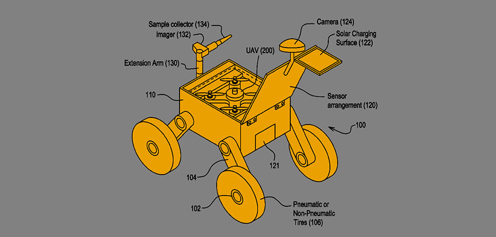
Dallas-Fort Worth ranked No. 9 for patents out of 250 metros. Patents granted include: 7-Eleven's object tracking system, Accenture's cost of healthcare analytics platform, American Airlines' flight number optimization system, Deere's scouting system with an autonomous ground vehicle, Mavenir Networks' system for supporting low latency applications in a cloud RAN, Roka Sports' snap-in nose pads for eyewear, The Parking Genius' sensors capable of determining direction and speed of vehicle entering or leaving a lot, and Toyota's system for monitoring suspicious activity of a vehicle.
-
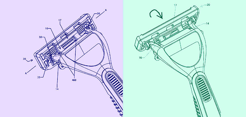
Dallas-Fort Worth ranked No. 9 for patents out of 250 metros. Patents granted include: Astrapi's methods of transmitting data using polynomial-based signals, AT&T's allocation and extraction of data for augmented reality for 6G or other next-gen network, Building Materials Investment Corp.'s moisture sensing roofing systems, COEVAC's automatic smoke/carbon monoxide evacuation system, IBM's cognitive intervention for voice recognition failure, Kioma's child safety seat, SanDisk Technologies' low latency data transfer, Shavelogic's shaving systems, USAA's recommendation engine for cost of a claim, and an unassigned virus immune computer system.
-
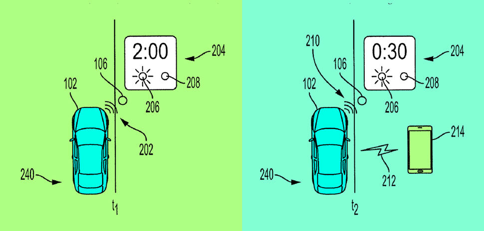
Dallas-Fort Worth ranked No. 11 for patents out of 250 metros. Patents granted include: Bank of America's authentication using blockchains, Dell's validation of data integrity through watermarking, Samsung's compensating for a movement of a sensor attached to a body of a user, SYNERGEN Technology Labs' baby monitor system sound and light delivery based on vitals,Toyota's parking meter monitoring and payment system, and Walmart's product recognition through multi-model image processing.
-
Dallas-Fort Worth ranked No. 11 for patents out of 250 metros. Patents granted include: Allied Bioscience's aqueous antimicrobial coatings, American Leather Operations convertible furniture, Caris Science's method for measuring the amount of at least one molecule in a bio sample, Siemens Industry Software 's environmental perception in autonomous driving STMicroelectronics' NFC antenna switch, Toyota's collaboorative robot hand bearing for high-torque tightening applications, and vSpatial's method for creating a collaborative virtual session.