
 Dallas Invents is a weekly look at U.S. patents granted with a connection to the Dallas-Fort Worth-Arlington metro area. Listings include patents granted to local assignees and/or those with a North Texas inventor. Patent activity can be an indicator of future economic growth, as well as the development of emerging markets and talent attraction. By tracking both inventors and assignees in the region, we aim to provide a broader view of the region’s inventive activity. Listings are organized by Cooperative Patent Classification (CPC).
THIS WEEK, BY THE NUMBERS
Week of July 16, 2019 | Dallas-Fort Worth-Arlington (19100)
156 patents granted
Ranked No. 11 in patent production out of 250 metros
NO. OF PATENTS BY CLASSIFICATION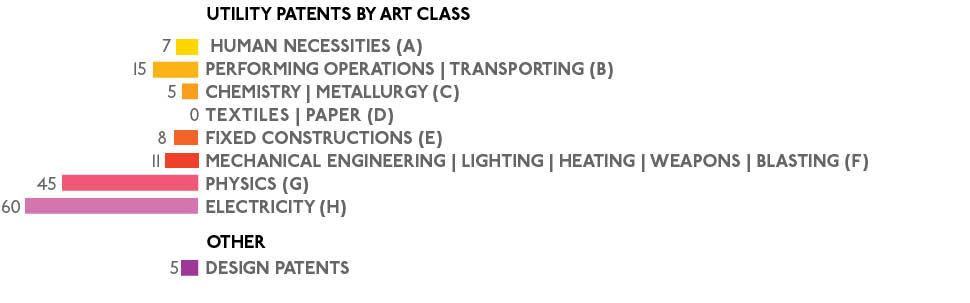
TOP LOCAL ASSIGNEES (NO. OF PATENTS)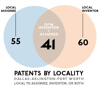
Sandisk Technologies LLC (Addison) 17
Texas Instruments Inc. (Dallas) 14
Futurewei Technologies Inc. (Plano) 10
Toyota Motor Engineering Manufacturing North America Inc. (Plano) 8
STMicroelectronics (Coppell) 5
CPG Technologies, LLC (Italy) 3
Bell Helicopter Textron Inc. (Fort Worth) 2
UNASSIGNED 13
TOP LOCAL INVENTOR (NO. OF PATENTS)
NA
FIRST SEEN
(COMPANIES THAT MAY BE ORIGINATING A PATENT IN DFW FOR THE FIRST TIME IN 2019, ACCORDING TO PATENT INDEX.)
Innovation Collective
Patent No. 10354288
System for apportioning revenue for media content derived from an online feedback community
Integrity Bio-Chemicals
Patent No. 10351770
Compositions and methods for the stabilization of clay-containing soils
Omega Acquisition
Patent No. 10355431
Consolidated automotive pigtail connector and replacement parts kit
Taiga Coolers
Patent No. 10350801
System and method for production of customized food and beverage coolers
The Pure Company Global
Patent No. D0854134
Air purifier
WoundKair Concepts
Patent No. D0854174
Cast shoe for a walking heel
Don’t miss Dallas Invents: Sign up for the Dallas Innovates e-newsletter. Patent information is provided by Joe Chiarella, founder of patent analytics company Patent Index and publisher of The Inventiveness Index.
For additional details on the patents granted below, search the USPTO Patent Full-Text and Image Database.
UTILITY PATENTS
H U M A N N E C E S S I T I E S
Thumb brace
Patent No. 10349692
Inventor(s): Hugh Allen Frederick (Dallas, TX)
Assignee(s): UNASSIGNED
Law Firm: Conley Rose, P.C. (3 non-local offices)
Application No., Date, Speed: 15284768 on 10/04/2016 (1015 days app to issue)
Abstract: A thumb brace comprising a glove having a thumb portion disposed between a palm side and a back side and comprising a first attachment region positioned adjacent a base of the thumb portion and a second attachment region positioned on the back side of the glove; a first elastic strap having a first end, a mid-portion, and a second end, wherein the mid-portion is disposed within a cradle of the glove between the thumb portion and an index finger portion of the glove, the first end is releasably attached to the first attachment region, and the second end is releasably attached to the first attachment region, whereby the first strap extends a distal end of a thumb metacarpal bone of a user of the brace; and a second elastic strap having a first end, a mid-portion, and a second end, wherein the first end is attached to the palm side of the glove and the second end is releasably attached to the second attachment region, whereby the second strap reduces a proximal end of a thumb metacarpal bone of a user of the brace.
[A41D] OUTERWEAR; PROTECTIVE GARMENTS; ACCESSORIES (eye or ear protectors A61F 9/00, A61F 11/00; sweating suits A61H 36/00)
Shaving razor tray
Patent No. 10349719
Inventor(s): Craig A. Provost (Boston, MA), John W. Griffin (Moultonborough, NH), William E. Tucker (Attleboro, MA)
Assignee(s): ShaveLogic, Inc. (Dallas, TX)
Law Firm: Leber IP Law (2 non-local offices)
Application No., Date, Speed: 16115157 on 08/28/2018 (322 days app to issue)
Abstract: A tray is disclosed for securely holding a shaving razor and a shaving cartridge magazine when not in use.
[A45D] HAIRDRESSING OR SHAVING EQUIPMENT; MANICURING OR OTHER COSMETIC TREATMENT (wigs, toupees, or the like A41G 3/00, A41G 5/00; hairdressers’ chairs A47C 1/04; hair cutting appliances, razors B26B)
Methods of designing and manufacturing customized dental prosthesis for periodontal or osseointegration and related systems
Patent No. 10350030
Inventor(s): Lea Ellermeier Nesbit (Dallas, TX)
Assignee(s): NATURAL DENTAL IMPLANTS AG (Berlin, , DE)
Law Firm: Bracewell LLP (3 non-local offices)
Application No., Date, Speed: 15376051 on 12/12/2016 (946 days app to issue)
Abstract: Methods of manufacturing dental prosthesis/implants each to replace a non-functional natural tooth positioned in a jawbone of a specific pre-identified patient are provided. An example method includes the steps of receiving imaging data such as x-ray image data and surface scan data of a dental anatomy and/or a physical impression of the dental anatomy of a specific preidentified patient. The steps can also include forming a three-dimensional virtual model of at least portions of a non-functional natural tooth positioned in the jawbone of the specific pre-identified patient based on the imaging and surface scan data, virtually designing a dental implant based upon the virtual model, exporting the data describing the designed dental implant to a manufacturing machine, and custom manufacturing the dental implant for the specific patient.
[A61C] DENTISTRY; APPARATUS OR METHODS FOR ORAL OR DENTAL HYGIENE (non-driven toothbrushes A46B; preparations for dentistry A61K 6/00; preparations for cleaning the teeth or mouth A61K 8/00, A61Q 11/00)
Medicinal drops
Patent No. 10350232
Inventor(s): Peter D. Jaillet (Lewisville, TX)
Assignee(s): UNASSIGNED
Law Firm: Chalker Flores, LLP (Local)
Application No., Date, Speed: 14527870 on 10/30/2014 (1720 days app to issue)
Abstract: The present invention includes a concentration of at least 7.5% w/w saccharide other than trehalose, a preservative, in a buffered solution, wherein the composition is formulated for optic or otic administration. In certain embodiments, the composition is used to treat dry eyes, presbyopia, eye pain, blurred vision, confused mental function, scotoma, allergies, reduced craving for sugar, blocked tear ducts, tremors, vision and cognitive changes due to concussion, vertigo, TBI, loss of cognitive function as a result of traumatic brain injury, multiple sclerosis, Parkinson”s disease, Alzheimer”s disease, attention deficit disorder, attention deficit hyperactivity disorder, or Guillain-Barre syndrome.
[A61K] PREPARATIONS FOR MEDICAL, DENTAL, OR TOILET PURPOSES (devices or methods specially adapted for bringing pharmaceutical products into particular physical or administering forms A61J 3/00; chemical aspects of, or use of materials for deodorisation of air, for disinfection or sterilisation, or for bandages, dressings, absorbent pads or surgical articles A61L; soap compositions C11D)
Methods of preparing ophthalmic formulations and uses of same
Patent No. 10350309
Inventor(s): Gerald D. Cagle (Fort Worth, TX), Haresh Bhagat (Fort Worth, TX)
Assignee(s): Cognoptix, Inc. (Concord, MA)
Law Firm: Hamilton, Brook, Smith Reynolds, P.C. (2 non-local offices)
Application No., Date, Speed: 15864679 on 01/08/2018 (554 days app to issue)
Abstract:
[A61K] PREPARATIONS FOR MEDICAL, DENTAL, OR TOILET PURPOSES (devices or methods specially adapted for bringing pharmaceutical products into particular physical or administering forms A61J 3/00; chemical aspects of, or use of materials for deodorisation of air, for disinfection or sterilisation, or for bandages, dressings, absorbent pads or surgical articles A61L; soap compositions C11D)
Amphibious aircraft fire fighting enhancement
Patent No. 10350441
Inventor(s): Marc A. Gerth (Keller, TX), Michael C. Story (Mansfield, TX), Reagan G. Bullock (Poolville, TX), Victor D. Trotter (Fort Worth, TX)
Assignee(s): GelTech Solutions, Inc. (Jupiter, FL)
Law Firm: McHale Slavin, P.A. (1 non-local offices)
Application No., Date, Speed: 15243367 on 08/22/2016 (1058 days app to issue)
Abstract: The instant invention relates to an apparatus and method for enhancing the fire extinguishing properties of water for use with fire fighting aircraft. The apparatus and method includes the steps of, and equipment for, transferring media into a holding tank in aircraft; filling a reservoir hopper with water in the aircraft; calculating the amount of media to be added to the reservoir; drawing the calculated amount of media into the reservoir to form an enhanced fire fighting admixture while the aircraft is in flight, wherein the admixture is offloaded by a controlled discharge for use in fighting forest fires.
[A62C] FIRE-FIGHTING (fire-extinguishing compositions, use of chemical substances in extinguishing fires A62D 1/00; spraying, applying liquids or other fluent materials to surfaces in general B05; fire-fighting aircraft B64D 1/16; alarm arrangements G08B, e.g. fire alarms actuated by smoke or gases G08B 17/10)
Golf club head with molded cavity structure
Patent No. 10350465
Inventor(s): Eric Larson (Arlington, TX), Randy Garrido (Fort Worth, TX)
Assignee(s): Karsten Manufacturing Corporation (Phoenix, AZ)
Law Firm: No Counsel
Application No., Date, Speed: 15815438 on 11/16/2017 (607 days app to issue)
Abstract: A golf club head includes a strike face, a crown, and a sole, and is formed from a forward section and a body section that are coupled together. The forward section includes the strike face, and the body section includes an upper shell defining a portion of the crown, a lower shell defining a portion of the sole, and an internal wall extending between the upper shell and the lower shell. The internal wall is molded from a polymeric material and is integrally formed with one of the upper shell and the lower shell. At least one of the upper shell and the lower shell defines an opening that is in communication with a cavity provided between the upper shell and the lower shell and at least partially defined by the internal wall.
[A63B] APPARATUS FOR PHYSICAL TRAINING, GYMNASTICS, SWIMMING, CLIMBING, OR FENCING; BALL GAMES; TRAINING EQUIPMENT (apparatus for passive exercising, massage A61H)
O P E R A T I O N S & T R A N S P O R T
Magnetic attachment for shaving cartridge
Patent No. 10350774
Inventor(s): Craig A. Provost (Providence, RI), John W. Griffin (Moultonborough, NH), Robert A. Wilson (Dallas, TX)
Assignee(s): SHAVELOGIC, INC. (Dallas, TX)
Law Firm: Leber IP Law (2 non-local offices)
Application No., Date, Speed: 14270792 on 05/06/2014 (1897 days app to issue)
Abstract: Shaving systems are disclosed that include a replaceable shaving assembly and a cartridge connecting structure for connecting the shaving assembly to a handle. In preferred implementations, the cartridge connecting structure has a magnetic portion configured to help draw the cartridge onto the handle and retain the cartridge in place when the razor is not in contact with the skin, and a mechanical engagement that provides the necessary retention forces required to keep the system intact during shaving.
[B26B] HAND-HELD CUTTING TOOLS NOT OTHERWISE PROVIDED FOR (for harvesting A01D; for horticulture, for forestry A01G; for butchering or meat treatment A22; for manufacturing or repairing footwear A43D; nail clippers or cutters A45D 29/02; kitchen equipment A47J; for surgical purposes A61B 17/00; for metal B23D; cutting by abrasive fluid jets B24C 5/02; plier-like tools with cutting edges B25B 7/22; pincers B25C 11/02; handles for hand implements, in general B25G; guillotine-type cutters B26D; for erasing B43L 19/00; for textile materials D06H)
Method of manufacturing a tray table
Patent No. 10350800
Inventor(s): William H. Maslakow (Lewisville, TX)
Assignee(s): Reliant Worldwide Plastics, LLC (Plano, TX)
Law Firm: Braxton Perrone, PLLC (1 non-local offices)
Application No., Date, Speed: 15178386 on 06/09/2016 (1132 days app to issue)
Abstract: Disclosed embodiments relate to trays typically comprising a composite internal structure, a thermoplastic frame typically located about the composite internal structure, and two cover sheets forming the upper and lower tray surfaces. The composite internal structure may be a corrugated composite structure in some embodiments. In other embodiments, the composite internal structure may comprise a series of composite elements (which might act a beams or struts). The cover sheets may comprise thermoplastic material, and in some embodiments, the cover sheets may comprise composite material (for example the same as for the corrugated composite structure). In some exemplary embodiments, the thermoplastic frame and the composite internal structure may have the same thermoplastic material, and they may be joined together to have a plurality of homogeneous connective attachments.
[B29C] SHAPING OR JOINING OF PLASTICS; SHAPING OF MATERIAL IN A PLASTIC STATE, NOT OTHERWISE PROVIDED FOR; AFTER-TREATMENT OF THE SHAPED PRODUCTS, e.g. REPAIRING (making preforms B29B 11/00; making laminated products by combining previously unconnected layers which become one product whose layers will remain together B32B 37/00-B32B 41/00) [4]
System and method for production of customized food and beverage coolers
Patent No. 10350801
Inventor(s): John S. Hohenshelt (Arlington, TX)
Assignee(s): Taiga Coolers, LLC (Arlington, TX)
Law Firm: Griggs Bergen LLP (Local)
Application No., Date, Speed: 14982836 on 12/29/2015 (1295 days app to issue)
Abstract: A system and method for production of a customizable food and beverage cooler are disclosed. In one embodiment of the system, a mold includes two primary halves configured to produce an injection molded part that is a component of the food and beverage cooler. An aperture intersects one of the primary halves of the mold to accommodate an insertion block that includes a reverse image thereon such that molten plastic flow around the reverse image produces an integrally molded image on the component of the food and beverage cooler. Further, the aperture accommodates a combination insertion block and insertion plate having the reverse image thereon. One of the insertion block or combination insertion block and insertion plate is selected for disposing in the aperture based on the desired production run of the injection molded part.
[B29C] SHAPING OR JOINING OF PLASTICS; SHAPING OF MATERIAL IN A PLASTIC STATE, NOT OTHERWISE PROVIDED FOR; AFTER-TREATMENT OF THE SHAPED PRODUCTS, e.g. REPAIRING (making preforms B29B 11/00; making laminated products by combining previously unconnected layers which become one product whose layers will remain together B32B 37/00-B32B 41/00) [4]
Apparatus and method for forming a polymeric web
Patent No. 10350806
Inventor(s): Brad A. Cobler (Irving, TX), Gregory James Wood (Carrollton, TX)
Assignee(s): Poly-America, L.P. (Grand Prairie, TX)
Law Firm: No Counsel
Application No., Date, Speed: 15075689 on 03/21/2016 (1212 days app to issue)
Abstract: The present invention is directed to an apparatus for forming a multi-layer web formed from at least two polymeric film tubes in intimate contact with each other but not bonded to each other. The apparatus and method includes the use of a blown film extrusion die that extrudes two separate blown film polymeric tubes via two separate annular die lips. A fluid cooling system applies cooling fluid across a plurality of surfaces of the two blown film tubes. One of the die lips may be at a different height from the other die lip. The frost line of one blown film tube may be at a different height from the other blown film tube.
[B29C] SHAPING OR JOINING OF PLASTICS; SHAPING OF MATERIAL IN A PLASTIC STATE, NOT OTHERWISE PROVIDED FOR; AFTER-TREATMENT OF THE SHAPED PRODUCTS, e.g. REPAIRING (making preforms B29B 11/00; making laminated products by combining previously unconnected layers which become one product whose layers will remain together B32B 37/00-B32B 41/00) [4]
Plastic processing screw
Patent No. 10350809
Inventor(s): Robert F. Dray, Sr. (Dallas, TX)
Assignee(s): UNASSIGNED
Law Firm: No Counsel
Application No., Date, Speed: 15134768 on 04/21/2016 (1181 days app to issue)
Abstract: An improved screw has a shaft having a surface and a central axis and at least one flight extending helically along the surface of the shaft in successive turns. A continuous groove is formed in the surface of the shaft and extends between successive, pushing and trailing, turns of the flight at a selected angle greater than zero. The groove defines at least one generally triangular land having a base aligned with a pushing turn of the flight and an apex between successive turns of the flight. The groove also defines another generally triangular land having a base aligned with a trailing turn of the flight. Barriers or dams may be provided on the lands and in the grooves. A second continuous groove may also be formed in the surface of the shaft.
[B29C] SHAPING OR JOINING OF PLASTICS; SHAPING OF MATERIAL IN A PLASTIC STATE, NOT OTHERWISE PROVIDED FOR; AFTER-TREATMENT OF THE SHAPED PRODUCTS, e.g. REPAIRING (making preforms B29B 11/00; making laminated products by combining previously unconnected layers which become one product whose layers will remain together B32B 37/00-B32B 41/00) [4]
Cloaking devices constructed from reflection boundaries and half-mirrors and vehicles comprising the same
Patent No. 10351062
Inventor(s): Chengang Ji (Ann Arbor, MI), Debasish Banerjee (Ann Arbor, MI), Kyu-Tae Lee (Ann Arbor, MI), Songtao Wu (Ann Arbor, MI)
Assignee(s): TOYOTA MOTOR ENGINEERING MANUFACTURING NORTH AMERICA, INC. (Plano, TX)
Law Firm: Dinsmore Shohl LLP (14 non-local offices)
Application No., Date, Speed: 15813830 on 11/15/2017 (608 days app to issue)
Abstract: A cloaking device includes an object-side, an image-side, and a cloaked region (CR) between the object-side and the image-side. An object-side CR reflection boundary, an object-side half-mirror, and an object-side external reflection boundary are positioned on the object-side, and an image-side CR reflection boundary, an image-side half-mirror, and an image-side external reflection boundary are positioned on the image-side. The object-side half-mirror and the object-side external reflection boundary are spaced apart and generally parallel to the object-side CR reflection boundary, and the image-side half-mirror and the image-side external reflection boundary are spaced apart and generally parallel to the image-side CR reflection boundary. Light from an object located on the object-side of the cloaking device and obscured by the CR is redirected around the CR via two optical paths to form an image of the object on the image-side of the cloaking device.
[B60R] VEHICLES, VEHICLE FITTINGS, OR VEHICLE PARTS, NOT OTHERWISE PROVIDED FOR (fire prevention, containment or extinguishing specially adapted for vehicles A62C 3/07)
License plate tag method and apparatus
Patent No. 10351079
Inventor(s): Andrey Korneev (Arlington, TX)
Assignee(s): UNASSIGNED
Law Firm: Law Office of Jeff Williams PLLC (Local + 690 other metros)
Application No., Date, Speed: 14967296 on 12/12/2015 (1312 days app to issue)
Abstract: A method of attaching a vehicular identification member to a vehicle performed by obtaining a vehicle identification member having selectively identifying information regarding the vehicle. Locating the identification member adjacent a surface of the vehicle. Using an attachment member to secure the vehicle identification member to the vehicle. The attachment member is at least one of or both an adhesive layer and a fastener slot. The vehicle identification member may be secured through the application of force through a fastener within the slot and bonding via the removable adhesive layer to an interior or exterior surface.
[B60R] VEHICLES, VEHICLE FITTINGS, OR VEHICLE PARTS, NOT OTHERWISE PROVIDED FOR (fire prevention, containment or extinguishing specially adapted for vehicles A62C 3/07)
Automatic brake application for one pedal driving
Patent No. 10351111
Inventor(s): Mariano Hernandez (Los Angeles, CA)
Assignee(s): TOYOTA MOTOR ENGINEERING MANUFACTURING NORTH AMERICA, INC. (Plano, TX)
Law Firm: Snell Wilmer LLP (5 non-local offices)
Application No., Date, Speed: 15493016 on 04/20/2017 (817 days app to issue)
Abstract: Methods, systems, and apparatus for controlling the braking of a vehicle. The brake control system includes a first sensor for detecting motion data of the vehicle and an electronic control unit connected to the first sensor. The electronic control unit is configured to determine that the vehicle is not in motion based on the motion data. The electronic control unit is configured to predict a brake application event that requires application of a braking force to prevent the vehicle from moving and cause brakes of the vehicle to apply the braking force to prevent the vehicle from moving based on the brake application event.
[B60T] VEHICLE BRAKE CONTROL SYSTEMS OR PARTS THEREOF; BRAKE CONTROL SYSTEMS OR PARTS THEREOF, IN GENERAL (control of electrodynamic brake systems B60L 7/00; conjoint control of brakes and other drive units of vehicles B60W); ARRANGEMENT OF BRAKING ELEMENTS ON VEHICLES IN GENERAL; PORTABLE DEVICES FOR PREVENTING UNWANTED MOVEMENT OF VEHICLES; VEHICLE MODIFICATIONS TO FACILITATE COOLING OF BRAKES [2006.01]
Apparatuses and methods for testing vehicle stone chipping
Patent No. 10351112
Inventor(s): Kevin C. Nevaux (Ann Arbor, MI)
Assignee(s): TOYOTA MOTOR ENGINEERING MANUFACTURING NORTH AMERICA, INC. (Plano, TX)
Law Firm: Dinsmore Shohl LLP (14 non-local offices)
Application No., Date, Speed: 15421670 on 02/01/2017 (895 days app to issue)
Abstract: An apparatus for testing vehicle stone chippings is disclosed. The apparatus includes a stone chipping rig having a chassis. The chassis includes a first end, a second end, and a longitudinally extending tongue extending from the second end. A rolling fixture is coupled to the first end of the chassis. A stone chipping test device is coupled to the first end of the chassis adjacent to the rolling fixture for measuring an impact force of a stone that strikes the stone chipping test device. The apparatus further includes a pilot vehicle used to receive the stone chipping rig so as to measure the impact force of the stone launched off the pilot vehicle wheels when the pilot vehicle travels on a road with loose gravel. The stone chipping rig is defined as a test vehicle towed at a fixed distance behind the pilot vehicle.
[B60T] VEHICLE BRAKE CONTROL SYSTEMS OR PARTS THEREOF; BRAKE CONTROL SYSTEMS OR PARTS THEREOF, IN GENERAL (control of electrodynamic brake systems B60L 7/00; conjoint control of brakes and other drive units of vehicles B60W); ARRANGEMENT OF BRAKING ELEMENTS ON VEHICLES IN GENERAL; PORTABLE DEVICES FOR PREVENTING UNWANTED MOVEMENT OF VEHICLES; VEHICLE MODIFICATIONS TO FACILITATE COOLING OF BRAKES [2006.01]
Electrically powered downlock actuation system
Patent No. 10351227
Inventor(s): Adam J. Ditzler (Fort Worth, TX)
Assignee(s): GOODRICH CORPORATION (Charlotte, NC)
Law Firm: Snell Wilmer, L.L.P. (3 non-local offices)
Application No., Date, Speed: 15224161 on 07/29/2016 (1082 days app to issue)
Abstract: A locking linkage system may comprise a lockable assembly comprising an upper brace, a lower brace coupled to the upper brace, and a linkage coupled to the upper brace and the lower brace. The locking linkage system may further comprise a downlock actuator comprising an electric motor coupled to the upper brace, a rotary output shaft coupled to the electric motor, a connecting output coupled to the rotary output shaft, wherein the connecting output shaft is configured to rotate between a fixed locked position and a fixed unlocked position, and a link rod having a distal end coupled to the linkage and a proximal end comprising a lost-motion joint, the lost-motion joint being coupled to a connection pin of connecting output shaft. The downlock actuator may be configured to toggle the linkage, the upper brace, and the lower brace between an unlocked position and a locked position.
[B64C] AEROPLANES; HELICOPTERS (air-cushion vehicles B60V)
Rotor assembly having collective pitch control
Patent No. 10351232
Inventor(s): John Richard McCullough (Fort Worth, TX), Paul K. Oldroyd (Fort Worth, TX)
Assignee(s): Bell Helicopter Textron Inc. (Fort Worth, TX)
Law Firm: Lawrence Youst PLLC (Local)
Application No., Date, Speed: 15606257 on 05/26/2017 (781 days app to issue)
Abstract: A rotor assembly for an aircraft operable to generate a variable thrust output at a constant rotational speed. The rotor assembly includes a mast rotatable at the constant speed about a mast axis. A rotor hub is coupled to and rotatable with the mast. The rotor hub includes a plurality of spindle grips extending generally radially outwardly. Each of the spindle grips is coupled to one of a plurality of rotor blades and is operable to rotate therewith about a pitch change axis. A collective pitch control mechanism is coupled to and rotatable with the rotor hub. The collective pitch control mechanism is operably associated with each spindle grip such that actuation of the collective pitch control mechanism rotates each spindle grip about the respective pitch change axis to collectively control the pitch of the rotor blades, thereby generating the variable thrust output.
[B64C] AEROPLANES; HELICOPTERS (air-cushion vehicles B60V)
Process for making a capsule containing a dosing agent
Patent No. 10351277
Inventor(s): Dennis Dwight Paynter (Grapevine, TX)
Assignee(s): 2266170 Ontario Inc. (Mississauga, ON, , CA)
Law Firm: Manelli Selter PLLC (2 non-local offices)
Application No., Date, Speed: 15224706 on 08/01/2016 (1079 days app to issue)
Abstract: A capsule is provided containing a dosing agent and a system and process is provided for making capsules containing a dosing agent. The capsule includes a body defining an interior space and an opening, the capsule having ingredients and a dosing agent disposed in the interior space and a cover to seal the opening. The process and system includes depositing ingredients and the dosing agent in the interior space of the capsule and then covering the opening.
[B65B] MACHINES, APPARATUS OR DEVICES FOR, OR METHODS OF, PACKAGING ARTICLES OR MATERIALS; UNPACKING (bundling and pressing devices for cigars A24C 1/44; devices for tensioning and securing binders adapted to be supported by the article or articles to be bound B25B 25/00; applying closure members to bottles, jars or similar containers B67B 1/00-B67B 6/00; concurrent cleaning, filling and closing of bottles B67C 7/00; emptying bottles, jars, cans, casks, barrels or similar containers B67C 9/00)
Method of manufacturing fiberglass filtration media
Patent No. 10351462
Inventor(s): Charles Douglas Spitler (Southlake, TX)
Assignee(s): Superior Fibers, LLC (Reedsville, WV)
Law Firm: Bakos Kritzer (2 non-local offices)
Application No., Date, Speed: 15255136 on 09/01/2016 (1048 days app to issue)
Abstract: The manufacture of fiberglass filtration media, and particularly paint arrestance fiberglass media, is disclosed. Fiberglass filtration media is formed in part by controlling the speed of a melter traversing a drum. The fiberglass media passes through rollers and water sprays before it enters a curing apparatus. Progressive density changes from the air intake side to the air exit side of the media result in increased filtration qualities.
[B01D] SEPARATION (separating solids from solids by wet methods B03B, B03D, by pneumatic jigs or tables B03B, by other dry methods B07; magnetic or electrostatic separation of solid materials from solid materials or fluids, separation by high-voltage electric fields B03C; centrifuges B04B; vortex apparatus B04C; presses per se for squeezing-out liquid from liquid-containing material B30B 9/02) [5]
System and method for detection of vehicle lane departure
Patent No. 10352704
Inventor(s): Vladimeros Vladimerou (Whitmore Lake, MI)
Assignee(s): Toyota Motor Engineering Manufacturing North America, Inc. (Plano, TX)
Law Firm: Darrow Mustafa PC (2 non-local offices)
Application No., Date, Speed: 16018686 on 06/26/2018 (385 days app to issue)
Abstract: A lane departure detection computing device for a roadside device is disclosed. The computing device is configured to execute instructions stored in a memory to: calculate a first path geometry relating to a first vehicle traveling in a first lane; calculate a second path geometry relating to a second vehicle traveling in a second lane different from the first lane; evaluate coextensive portions of the first path geometry and the second path geometry for parallelism; if the coextensive portions of the first path geometry and the second path geometry evaluated for parallelism are not parallel, determine that one of the first vehicle and the second vehicle is executing a lane departure; and operate a vehicle configured for autonomous operation responsive to the determination that one of the first vehicle and the second vehicle is executing a lane departure.
[B60W] CONJOINT CONTROL OF VEHICLE SUB-UNITS OF DIFFERENT TYPE OR DIFFERENT FUNCTION; CONTROL SYSTEMS SPECIALLY ADAPTED FOR HYBRID VEHICLES; ROAD VEHICLE DRIVE CONTROL SYSTEMS FOR PURPOSES NOT RELATED TO THE CONTROL OF A PARTICULAR SUB-UNIT [2006.01]
Process for forming PZT or PLZT thinfilms with low defectivity
Patent No. 10354858
Inventor(s): Asad Mahmood Haider (Plano, TX), John Britton Robbins (McKinney, TX)
Assignee(s): TEXAS INSTRUMENTS INCORPORATED (Dallas, TX)
Law Firm: No Counsel
Application No., Date, Speed: 14467688 on 08/25/2014 (1786 days app to issue)
Abstract: Use of a non-solvent for the edge bead removal of spin-coated PZT or PLZT thinfilms, eliminates swelling of the exposed edges of the PZT or PLZT thinfilms and eliminates delamination and formation of particle defects in subsequent bake and anneal steps.
[B05D] PROCESSES FOR APPLYING LIQUIDS OR OTHER FLUENT MATERIALS TO SURFACES, IN GENERAL (conveying articles or workpieces through baths of liquid B65G, e.g. B65G 49/02) [2]
C H E M I S T R Y & M E T A L L U R G Y
Composition and method for inhibiting corrosion
Patent No. 10351453
Inventor(s): Lyle H. Steimel (Flower Mound, TX), Marta Drewniak (Carrollton, TX)
Assignee(s): NCH Corporation (Irving, TX)
Law Firm: Ross Barnes LLP (1 non-local offices)
Application No., Date, Speed: 15273158 on 09/22/2016 (1027 days app to issue)
Abstract: A composition and method of inhibiting corrosion and white rust on metal components in a water system. The composition preferably comprises an amino-acid based polymer (most preferably a polyaspartic acid or a salt thereof), hydroxyphosphonoacetic acid, and a second phosphonic acid (preferably a phosphonocarboxylic acid), and does not require the use of regulated metals. The composition is effective even in the presence of biocides. A preferred method of inhibiting white rust comprises adding an amino-acid based polymer or hydroxyphosphonoacetic acid or both to the water system. A preferred method of inhibiting corrosion or white rust comprises adding an amino-acid based polymer, hydroxyphosphonoacetic acid, and a phosphonocarboxylic acid to the water system. Preferably the active concentrations are at least 3 ppm each of the amino-acid based polymer and hydroxyphosphonoacetic acid when added to a volume of water in the water system.
[C02F] TREATMENT OF WATER, WASTE WATER, SEWAGE, OR SLUDGE (processes for making harmful chemical substances harmless, or less harmful, by effecting a chemical change in the substances A62D 3/00; separation, settling tanks or filter devices B01D; special arrangements on waterborne vessels of installations for treating water, waste water or sewage, e.g. for producing fresh water, B63J; adding materials to water to prevent corrosion C23F; treating radioactively-contaminated liquids G21F 9/04) [3]
Graphite oxide entrainment in cement and asphalt composite
Patent No. 10351473
Inventor(s): Richard Stoltz (Plano, TX)
Assignee(s): Garmor Inc. (Orlando, FL)
Law Firm: Chalker Flores, LLP (Local)
Application No., Date, Speed: 15792322 on 10/24/2017 (630 days app to issue)
Abstract: A method of producing dispersed of high quality graphene/graphite oxides in a powder matrix to then be reacted to form a composite. Where the powders have similar hydrophobicity and the graphene/graphite oxides has minimal surface oxidation or minimal epoxy group and where the powders are sonically mixed.
[C01B] NON-METALLIC ELEMENTS; COMPOUNDS THEREOF (fermentation or enzyme-using processes for the preparation of elements or inorganic compounds except carbon dioxide C12P 3/00; production of non-metallic elements or inorganic compounds by electrolysis or electrophoresis C25B)
Engineered composite structure using graphene oxide
Patent No. 10351711
Inventor(s): Richard Stoltz (Plano, TX)
Assignee(s): UNASSIGNED
Law Firm: Chalker Flores, LLP (Local)
Application No., Date, Speed: 15559741 on 03/18/2016 (1215 days app to issue)
Abstract: This is generally a method of producing dispersed high quality engineered composite structures using flat flakes of graphene/graphene oxides/reduced graphene oxides in a host as the reinforcing additive of the composite.
[C09C] TREATMENT OF INORGANIC MATERIALS, OTHER THAN FIBROUS FILLERS, TO ENHANCE THEIR PIGMENTING OR FILLING PROPERTIES (preparation of inorganic compounds or non-metallic elements C01; treatment of materials specially adapted to enhance their filling properties in mortars, concrete or artificial stone C04B 14/00, C04B 18/00, C04B 20/00); PREPARATION OF CARBON BLACK [4]
Method of improving the accuracy when quantifying fluorescence markers in fuels
Patent No. 10351789
Inventor(s): Jeffrey L. Conroy (Allen, TX), Philip B. Forshee (McKinney, TX)
Assignee(s): Authentix, Inc. (Addison, TX)
Law Firm: Conley Rose, P.C. (3 non-local offices)
Application No., Date, Speed: 15632532 on 06/26/2017 (750 days app to issue)
Abstract: A method of increasing the accuracy of the quantification of an analyte in a hydrocarbon, the analyte containing a marking compound, by obtaining a first sample containing (a) the hydrocarbon and (b) the marking compound, obtaining a homogeneity inducing material, contacting the homogeneity inducing material with an aliquot of the first sample in a volumetric ratio of greater than or equal to about 5:1 to produce a second sample, and determining an amount of the marking compound in the second sample using an analytical technique based on the marking material.
[C10L] FUELS NOT OTHERWISE PROVIDED FOR; NATURAL GAS; SYNTHETIC NATURAL GAS OBTAINED BY PROCESSES NOT COVERED BY SUBCLASSES C10G OR C10K; LIQUEFIED PETROLEUM GAS; USE OF ADDITIVES TO FUELS OR FIRES; FIRE-LIGHTERS [5]
Methods for treatment of oncological disorders using an epimetabolic shifter (Coenzyme Q10)
Patent No. 10351915
Inventor(s): John Patrick McCook (Frisco, TX)
Assignee(s): UNASSIGNED
Law Firm: McCarter English, LLP (7 non-local offices)
Application No., Date, Speed: 15862856 on 01/05/2018 (557 days app to issue)
Abstract: Methods and formulations for treating onocological disorders in humans using Coenzyme Q10 are described.
[C12Q] MEASURING OR TESTING PROCESSES INVOLVING ENZYMES OR MICROORGANISMS (immunoassay G01N 33/53); COMPOSITIONS OR TEST PAPERS THEREFOR; PROCESSES OF PREPARING SUCH COMPOSITIONS; CONDITION-RESPONSIVE CONTROL IN MICROBIOLOGICAL OR ENZYMOLOGICAL PROCESSES [3]
F I X E D C O N S T R U C T I O N S
Compositions and methods for the stabilization of clay containing soils
Patent No. 10351770
Inventor(s): Ashoka V. R. Madduri (Belmont, MA), Charles E. Milliron, III (Columbus, GA), Curtis J. Rodencal (Cresson, TX), Matthew B. Blackmon (Columbus, GA), Sameer S. Vhora (Columbus, GA), Sanket Gandhi (Columbus, GA)
Assignee(s): Integrity Bio-Chemicals, LLC (Cresson, TX)
Law Firm: Vorys, Sater, Seymour and Pease LLP (5 non-local offices)
Application No., Date, Speed: 16054259 on 08/03/2018 (347 days app to issue)
Abstract: Polysaccharides may be partially oxidized by oxidative opening of a monosaccharide unit while still retaining glycosidic bonds. Such polysaccharides may be further functionalized with an amine moiety at a site of oxidative opening. Polysaccharides that are partially oxidized and amine-functionalized in this manner may be combined with an aqueous liquid to form compositions suitable for stabilizing clays in clay-containing formations. Clay stabilization may promote reduced swelling of the clays in the presence of water.
[E02D] FOUNDATIONS; EXCAVATIONS; EMBANKMENTS (specially adapted for hydraulic engineering E02B); UNDERGROUND OR UNDERWATER STRUCTURES [6]
Formation aids for use in forming swimming pools and associated method
Patent No. 10352055
Inventor(s): Brian Claffey (Colleyville, TX)
Assignee(s): UNASSIGNED
Law Firm: Braxton Perrone, PLLC (1 non-local offices)
Application No., Date, Speed: 15870564 on 01/12/2018 (550 days app to issue)
Abstract: A formation aid, for use in the forming of receptacles in a swimming pool, includes a three-dimensional body having an essentially conical shape. The three-dimensional body of the formation aid includes a narrow end, for placement near an interior edge of the swimming pool during formation of the swimming pool; and a wide end, for placement remote from the interior edge of the swimming pool, in order to form a receptacle.
[E04H] BUILDINGS OR LIKE STRUCTURES FOR PARTICULAR PURPOSES; SWIMMING OR SPLASH BATHS OR POOLS; MASTS; FENCING; TENTS OR CANOPIES, IN GENERAL (foundations E02D) [4]
Formation aids for use in forming swimming pools and associated method
Patent No. 10352056
Inventor(s): Brian Claffey (Colleyville, TX)
Assignee(s): UNASSIGNED
Law Firm: Braxton Perrone, PLLC (1 non-local offices)
Application No., Date, Speed: 16119273 on 08/31/2018 (319 days app to issue)
Abstract: A formation aid, for use in the forming of receptacles in a swimming pool, includes a three-dimensional body having an essentially conical shape. The three-dimensional body of the formation aid includes a narrow end, for placement near an interior edge of the swimming pool during formation of the swimming pool; and a wide end, for placement remote from the interior edge of the swimming pool, in order to form a receptacle.
[E04H] BUILDINGS OR LIKE STRUCTURES FOR PARTICULAR PURPOSES; SWIMMING OR SPLASH BATHS OR POOLS; MASTS; FENCING; TENTS OR CANOPIES, IN GENERAL (foundations E02D) [4]
Cutter support element
Patent No. 10352103
Inventor(s): Jason Maw (Beaumont, , CA)
Assignee(s): Ulterra Drilling Technologies, L.P. (Fort Worth, TX)
Law Firm: Kilpatrick Townsend Stockton LLP (14 non-local offices)
Application No., Date, Speed: 14338404 on 07/23/2014 (1819 days app to issue)
Abstract: Cutters mounted on bits for advancing boreholes are subject to extreme forces that can separate the cutter from the bit. A cutter backing element with a rearward extending lug and forward face can provide support to the cutter. The backing element is attached to the back face of the cutter and the lug of the backing element is received in a recess of the bit. The backing element can be brazed to the bit and the cutter. The lug is offset from a longitudinal axis of the backing element. Forces applied to the front of the cutter during drilling operations are transferred through the cutter to the backing element and to the bit through the offset lug.
[E21B] EARTH OR ROCK DRILLING (mining, quarrying E21C; making shafts, driving galleries or tunnels E21D); OBTAINING OIL, GAS, WATER, SOLUBLE OR MELTABLE MATERIALS OR A SLURRY OF MINERALS FROM WELLS [5]
Valve for use with downhole tools
Patent No. 10352131
Inventor(s): David Allen Dockweiler (Prosper, TX)
Assignee(s): Halliburton Energy Services, Inc. (Houston, TX)
Law Firm: McAfee Taft (7 non-local offices)
Application No., Date, Speed: 15518037 on 12/17/2014 (1672 days app to issue)
Abstract: An apparatus and method relating to down-hole production equipment for use in an oil well environment is provided. The apparatus and method are for selectively isolating fluid flow through a production packer or other down-hole tubular device. The apparatus and method use a ball valve, which is moved from an open position to a closed position by lateral or axial movement of the tubing string as opposed to by rotating the tubing string.
[E21B] EARTH OR ROCK DRILLING (mining, quarrying E21C; making shafts, driving galleries or tunnels E21D); OBTAINING OIL, GAS, WATER, SOLUBLE OR MELTABLE MATERIALS OR A SLURRY OF MINERALS FROM WELLS [5]
Removing liquid by subsurface compression system
Patent No. 10352137
Inventor(s): Kuo-Chiang Chen (Kennedale, TX)
Assignee(s): Upwing Energy, LLC (Cerritos, CA)
Law Firm: Fish Richardson P.C. (Local + 13 other metros)
Application No., Date, Speed: 16241673 on 01/07/2019 (190 days app to issue)
Abstract: A gas flow velocity within a horizontal wellbore section is increased by a velocity string and a downhole-type compressor. A pressure within the horizontal wellbore section is decreased by a downhole-type compressor located within a vertical wellbore section fluidically connected to the horizontal wellbore section. Liquid build-up within the horizontal wellbore section is decreased in response to the increased gas flow velocity and the decreased pressure.
[E21B] EARTH OR ROCK DRILLING (mining, quarrying E21C; making shafts, driving galleries or tunnels E21D); OBTAINING OIL, GAS, WATER, SOLUBLE OR MELTABLE MATERIALS OR A SLURRY OF MINERALS FROM WELLS [5]
Forming multilateral wells
Patent No. 10352140
Inventor(s): Joseph DeWitt Parlin (Plano, TX)
Assignee(s): Halliburton Energy Services, Inc. (Houston, TX)
Law Firm: Parker Justiss, P.C. (2 non-local offices)
Application No., Date, Speed: 15307080 on 05/29/2014 (1874 days app to issue)
Abstract: In one example of forming multilateral wells in unconventional reservoirs, a subterranean zone is drilled using a drilling rig to form a main wellbore. Using the drilling rig, the subterranean zone is drilled to form a lateral wellbore off the main wellbore. The drilling rig is removed after forming a multilateral well including the main wellbore and the lateral wellbore. Using a fracturing system, a fracture treatment is performed on the lateral wellbore.
[E21B] EARTH OR ROCK DRILLING (mining, quarrying E21C; making shafts, driving galleries or tunnels E21D); OBTAINING OIL, GAS, WATER, SOLUBLE OR MELTABLE MATERIALS OR A SLURRY OF MINERALS FROM WELLS [5]
Advanced perforation modeling
Patent No. 10352153
Inventor(s): John Hardesty (Weatherford, TX), Matthew Bell (Houston, TX), Sashi Gunturu (Katy, TX)
Assignee(s): GEODYNAMICS, INC. (Millsap, TX)
Law Firm: Patent Portfolio Builders PLLC (4 non-local offices)
Application No., Date, Speed: 14775977 on 03/14/2014 (1950 days app to issue)
Abstract: A technique is provided for modeling flow simulations at downhole reservoir conditions and rock formations after performing wellbore perforations. By utilizing these flow simulations, a user may be able to simulate and compare different scenarios, thereby facilitating a more effective, profitable, and realistic choice of perforating systems and operating conditions.
[E21B] EARTH OR ROCK DRILLING (mining, quarrying E21C; making shafts, driving galleries or tunnels E21D); OBTAINING OIL, GAS, WATER, SOLUBLE OR MELTABLE MATERIALS OR A SLURRY OF MINERALS FROM WELLS [5]
M E C H A N I C A L E N G I N E E R I N G
LIGHTING | HEATING | WEAPONS | BLASTING
Expander piston ring overlap protection and methods of use
Patent No. 10350739
Inventor(s): David W. Newberry (Gallipolis, OH)
Assignee(s): Toyota Motor Engineering Manufacturing North America (Plano, TX)
Law Firm: Dinsmore Shohl LLP (14 non-local offices)
Application No., Date, Speed: 15047979 on 02/19/2016 (1243 days app to issue)
Abstract: Methods and apparatuses for installing a piston ring onto a piston include a piston ring feeder having at least one projection feature and a receiving aperture. Methods include receiving a piston end having a piston groove into the receiving aperture until the piston groove is above piston rings on the piston ring feeder and below projection feature top ends; raising a ring to partially snap into the piston groove with ring ends separated by a first projection feature and the ring wrapped around a second projection feature; raising the piston such that the ring is pulled off the second projection feature while the first projection feature separates the ring ends; and raising the piston such that the first projection feature releases the ring ends and the ring fully snaps into the piston groove to form a gap between the ring ends of the ring seated in the piston groove.
[F16J] PISTONS; CYLINDERS; PRESSURE VESSELS IN GENERAL; SEALINGS
Reciprocating pump with dual circuit power end lubrication system
Patent No. 10352321
Inventor(s): Edward C. Kotapish (Willow Park, TX), Jacob A. Bayyouk (Richardson, TX), Joseph H. Byrne (Hudson Oaks, TX), Lawrence Waweru (Fort Worth, TX), Scott Skurdalsvold (Mansfield, TX)
Assignee(s): S.P.M. Flow Control, Inc. (Fort Worth, TX)
Law Firm: Foley Lardner LLP (Local + 13 other metros)
Application No., Date, Speed: 14808726 on 07/24/2015 (1453 days app to issue)
Abstract: A dual circuit lubrication system for a power end of a reciprocating pump that includes a lubrication pump that supplies lubrication fluid to a high pressure lubrication circuit and a low pressure lubrication circuit. The high pressure lubrication circuit is fluidly coupled to a crankshaft to supply lubrication fluid to sliding surfaces associated with the crankshaft at a first lubrication fluid pressure. The crankshaft drives a crosshead coupled to a plunger to displace fluid from a fluid end of the reciprocating pump. The low pressure lubrication circuit is fluidly coupled to supply the lubrication fluid to a plurality of rolling surfaces associated with the crankshaft at a second lubrication fluid pressure. The first lubrication fluid pressure is greater than the second lubrication fluid pressure.
[F04B] POSITIVE-DISPLACEMENT MACHINES FOR LIQUIDS; PUMPS (engine fuel-injection pumps F02M; machines for liquids, or pumps, of rotary-piston or oscillating-piston type F04C; non-positive-displacement pumps F04D; pumping of fluid by direct contact of another fluid or by using inertia of fluid to be pumped F04F; crankshafts, crossheads, connecting-rods F16C; flywheels F16F; gearings for interconverting rotary motion and reciprocating motion in general F16H; pistons, piston-rods, cylinders, in general F16J; ion pumps H01J 41/12; electrodynamic pumps H02K 44/02)
Crankshaft assembly
Patent No. 10352414
Inventor(s): Fred E. Hunstable (Granbury, TX)
Assignee(s): UNASSIGNED
Law Firm: No Counsel
Application No., Date, Speed: 15691382 on 08/30/2017 (685 days app to issue)
Abstract: There is presented various embodiments disclosed in this application, including an improved crankshaft system using a load connecting member which provides a greater maximum torque angle than a conventional system, thereby improving efficiency and power.
[F16H] GEARING
Integrated fuel pipe clamp with simple ergonomic fitting structure
Patent No. 10352490
Inventor(s): Eric F. Bursch (Ann Arbor, MI)
Assignee(s): TOYOTA MOTOR ENGINEERING MANUFACTURING NORTH AMERICA, INC. (Plano, TX)
Law Firm: Dinsmore Shohl LLP (14 non-local offices)
Application No., Date, Speed: 15219404 on 07/26/2016 (1085 days app to issue)
Abstract: An integrated clamp assembly for fluid tubes, a fluid tube assembly and a method of connecting automotive fuel tubes. The assembly includes a clamp body with side-by-side channels for receiving complementary-sized side-by-side fluid tubes, a clamp cover, numerous quick connectors to fluidly join the ends of fluid tubes together, and a retaining clip for each quick connector to keep the end of one of the joined fluid tubes secured to the quick connector. The size of the quick connectors is such that when placed within a corresponding section of the channel formed in the clamp body, the smaller quick connector length provides an axially-compliant fit within the respective channel. This compliance makes it easier for an installer, manufacturer, assembler or related personnel to fluidly connect the ends of axially-adjacent fluid tubes together within the clamp in situations where manufacturing tolerances cause one of the side-by-side fluid tubes that is to be secured by the quick connector and retaining clip to project a different length along a fluid flow dimension than that of its neighboring fluid tube.
[F16L] PIPES; JOINTS OR FITTINGS FOR PIPES; SUPPORTS FOR PIPES, CABLES OR PROTECTIVE TUBING; MEANS FOR THERMAL INSULATION IN GENERAL
Heating furnace using auto heating commissioning mode
Patent No. 10352572
Inventor(s): Eric M. Perez (Hickory Creek, TX), Mark G. Beste (Grapevine, TX), Steven Schneider (Plano, TX)
Assignee(s): Lennox Industries, Inc. (Richardson, TX)
Law Firm: Baker Botts L.L.P. (Local + 8 other metros)
Application No., Date, Speed: 15006604 on 01/26/2016 (1267 days app to issue)
Abstract: A heating control device including input/output ports, a memory operable to store smoke output thresholds, and a microprocessor. The microprocessor is configured to transmit a first electrical signal to operate an air circulation fan at a first speed and a heating unit in a first configuration to burn a lubricant at a first temperature where less than all of the burners are active. The microprocessor is further configured to obtain a smoke output measurement for the first temperature, compare the smoke output measurement to the smoke output threshold, and transmit a second electrical signal to transition the air circulation fan to a second speed to burn the lubricant at a second temperature that is greater than the first temperature when the smoke output measurement is less than the smoke output threshold and is less than the first temperature when the smoke output measurement is greater than the smoke output threshold.
[F24D] DOMESTIC- OR SPACE-HEATING SYSTEMS, e.g. CENTRAL HEATING SYSTEMS; DOMESTIC HOT-WATER SUPPLY SYSTEMS; ELEMENTS OR COMPONENTS THEREFOR (preventing corrosion C23F; water supply in general E03; using steam or condensate extracted or exhausted from steam engine plants for heating purposes F01K 17/02; steam traps F16T; domestic stoves or ranges F24B, F24C; water or air heaters having heat generating means F24H; combined heating and refrigeration systems F25B; heat exchange apparatus or elements F28; removing furring F28G; electric heating elements or arrangements H05B)
Method of and system for detecting loss of refrigerant charge
Patent No. 10352579
Inventor(s): David Omlor (Flower Mound, TX), LiYing Guo (Addison, TX)
Assignee(s): Lennox Industries Inc. (Richardson, TX)
Law Firm: Winstead PC (Local + 2 other metros)
Application No., Date, Speed: 15014286 on 02/03/2016 (1259 days app to issue)
Abstract: A method of determining loss of refrigerant charge in a heating, ventilation, and air conditioning (HVAC) system. The method includes receiving, using a controller, a plurality of temperature values from a plurality of temperature sensors placed at multiple locations within the HVAC system and calculating, using the controller using the plurality of temperature values, a plurality of temperature-dependent values. The method further includes determining, using the controller, whether a first temperature-dependent value of the plurality of temperature-dependent values is above a first predetermined temperature value and responsive to a determination that the first temperature-dependent value is above the first predetermined temperature value, transmitting, using the controller to a user interface, a notification indicating that the HVAC system is operating with low refrigerant charge.
[F25B] REFRIGERATION MACHINES, PLANTS, OR SYSTEMS; COMBINED HEATING AND REFRIGERATION SYSTEMS; HEAT PUMP SYSTEMS (heat-transfer, heat-exchange or heat-storage materials, e.g. refrigerants, or materials for the production of heat or cold by chemical reactions other than by combustion C09K 5/00; pumps, compressors F04; use of heat pumps for domestic or space-heating or for domestic hot-water supply F24D; air-conditioning, air-humidification F24F; fluid heaters using heat pumps F24H)
Defrost control using fan data
Patent No. 10352611
Inventor(s): H. Gene Havard (Carrollton, TX), Jeff Mangum (Argyle, TX), Jon Douglas (Lewisville, TX), Yi Qu (Coppell, TX)
Assignee(s): Lennox Industries Inc. (Richardson, TX)
Law Firm: Baker Botts L.L.P. (Local + 8 other metros)
Application No., Date, Speed: 15794782 on 10/26/2017 (628 days app to issue)
Abstract: In various implementations, frost in a vapor compression system may be controlled. A property of a fan may be determined. A determination may be made whether a frost event and/or a nonfrost event has occurred based at least partially on the determined fan property.
[F25B] REFRIGERATION MACHINES, PLANTS, OR SYSTEMS; COMBINED HEATING AND REFRIGERATION SYSTEMS; HEAT PUMP SYSTEMS (heat-transfer, heat-exchange or heat-storage materials, e.g. refrigerants, or materials for the production of heat or cold by chemical reactions other than by combustion C09K 5/00; pumps, compressors F04; use of heat pumps for domestic or space-heating or for domestic hot-water supply F24D; air-conditioning, air-humidification F24F; fluid heaters using heat pumps F24H)
Dual axial fan with a thermal exchange component for a vehicle
Patent No. 10352621
Inventor(s): Stephen William O”Brien (Fort Worth, TX)
Assignee(s): TSI Products, Inc. (Arlington, TX)
Law Firm: Hitchcock Evert LLP (Local)
Application No., Date, Speed: 14846427 on 09/04/2015 (1411 days app to issue)
Abstract: A dual fan apparatus for providing heated or cooled air which is compact fit within limited spaces. The dual fan apparatus includes two axial fans on opposing sides of a thermal exchange component which operate in coordination to move air in one direction at a time through the apparatus. The dual fan apparatus increases airflow and thermal transfer efficiency through the thermal exchange component.
[F28D] HEAT-EXCHANGE APPARATUS, NOT PROVIDED FOR IN ANOTHER SUBCLASS, IN WHICH THE HEAT-EXCHANGE MEDIA DO NOT COME INTO DIRECT CONTACT (heat-transfer, heat-exchange or heat-storage materials C09K 5/00; fluid heaters having heat generating means and heat transferring means F24H; furnaces F27; details of heat-exchange apparatus of general application F28F); HEAT STORAGE PLANTS OR APPARATUS IN GENERAL [4]
Method of making a primer insert for use in polymer ammunition
Patent No. 10352664
Inventor(s): Lonnie Burrow (Carrollton, TX)
Assignee(s): TRUE VELOCITY IP HOLDINGS, LLC (Garland, TX)
Law Firm: No Counsel
Application No., Date, Speed: 15911544 on 03/05/2018 (498 days app to issue)
Abstract: One embodiment of the present invention provides a polymeric ammunition cartridge and methods of making and using the same. The cartridge includes a substantially cylindrical insert connected to a substantially cylindrical polymeric middle body. The substantially cylindrical insert includes a top surface opposite a bottom surface and a substantially cylindrical coupling element that extends from the bottom surface, a primer recess in the top surface that extends toward the bottom surface, a primer flash hole positioned in the primer recess to extend through the bottom surface, and a flange that extends circumferentially about an outer edge of the top surface. The substantially cylindrical polymeric middle body includes a substantially cylindrical polymeric bullet-end and a substantially cylindrical polymeric coupling end connected by a powder chamber, wherein the substantially cylindrical polymeric coupling end extends over the substantially cylindrical coupling element and covers a circumferential surface of the primer flash hole.
[F42B] EXPLOSIVE CHARGES, e.g. FOR BLASTING; FIREWORKS; AMMUNITION (explosive compositions C06B; fuzes F42C; blasting F42D) [5]
Lightweight polymer ammunition cartridge casings
Patent No. 10352670
Inventor(s): Lonnie Burrow (Carrollton, TX)
Assignee(s): TRUE VELOCITY IP HOLDINGS, LLC (Garland, TX)
Law Firm: No Counsel
Application No., Date, Speed: 14320961 on 07/01/2014 (1841 days app to issue)
Abstract: One embodiment of the present invention provides a polymeric ammunition cartridge and methods of making and using the same. The cartridge includes a substantially cylindrical insert connected to a substantially cylindrical polymeric middle body. The substantially cylindrical insert includes a top surface opposite a bottom surface and a substantially cylindrical coupling element that extends from the bottom surface, a primer recess in the top surface that extends toward the bottom surface, a primer flash hole positioned in the primer recess to extend through the bottom surface, and a flange that extends circumferentially about an outer edge of the top surface. The substantially cylindrical polymeric middle body includes a substantially cylindrical polymeric bullet-end and a substantially cylindrical polymeric coupling end connected by a powder chamber, wherein the substantially cylindrical polymeric coupling end extends over the substantially cylindrical coupling element and covers a circumferential surface of the primer flash hole.
[F42B] EXPLOSIVE CHARGES, e.g. FOR BLASTING; FIREWORKS; AMMUNITION (explosive compositions C06B; fuzes F42C; blasting F42D) [5]
HVAC system detecting user discomfort
Patent No. 10353369
Inventor(s): Payam Delgoshaei (Addison, TX), Sridhar Venkatesh (Irving, TX)
Assignee(s): Lennox Industries, Inc. (Richardson, TX)
Law Firm: Baker Botts L.L.P. (Local + 8 other metros)
Application No., Date, Speed: 15655428 on 07/20/2017 (726 days app to issue)
Abstract: A controller for an HVAC system comprises an interface, a memory, and a processor. The interface receives data related to user interactions with the system, and receives a temperature of the enclosed space. The memory stores an accumulated user discomfort value and discomfort score values, associated with user interactions. The processor determines a difference between the enclosed space temperature and a setpoint temperature. The processor determines whether the temperature difference exceeds a first threshold, and in response to determining that, determine whether a user has interacted with the system. In response to determining that the user has interacted with the system, the processor determines a current user discomfort value based on the discomfort score values, updates the accumulated user discomfort value, and determines whether the accumulated user discomfort value exceeds a second threshold. In response to determining that, the processor generates an alert indicating that a user discomfort event has occurred.
[F24F] AIR-CONDITIONING; AIR-HUMIDIFICATION; VENTILATION; USE OF AIR CURRENTS FOR SCREENING (removing dirt or fumes from areas where they are produced B08B 15/00; vertical ducts for carrying away waste gases from buildings E04F 17/02; tops for chimneys or ventilating shafts, terminals for flues F23L 17/02)
P H Y S I C S
Cloaking devices with half Fresnel lenses and plane mirrors and vehicles comprising the same
Patent No. 10351063
Inventor(s): Chengang Ji (Ann Arbor, MI), Debasish Banerjee (Ann Arbor, MI), Kyu-Tae Lee (Ann Arbor, MI)
Assignee(s): TOYOTA MOTOR ENGINEERING MANUFACTURING NORTH AMERICA, INC. (Plano, TX)
Law Firm: Dinsmore Shohl LLP (14 non-local offices)
Application No., Date, Speed: 15863353 on 01/05/2018 (557 days app to issue)
Abstract: A cloaking device includes an object-side, an image-side and a cloaked region between the object side and image-side. An object-side half Fresnel lens, an image-side half Fresnel lens and a planar reflection boundary positioned between the object-side half Fresnel lens and the image-side half Fresnel lens are included. The object-side half Fresnel lens and the image-side half Fresnel lens each comprise an inward facing surface and an outward facing Fresnel surface. The planar reflection boundary comprises an inward facing mirror surface. Light from an object positioned on the object-side of the cloaking device and obscured by the cloaked region is redirected around the cloaked region by the object-side half Fresnel lens, planar reflection boundary and image-side half Fresnel lens to form an image of the object on the image-side of the cloaking device such that the light from the object appears to pass through the cloaked region.
[G02B] OPTICAL ELEMENTS, SYSTEMS, OR APPARATUS (G02F takes precedence; optical elements specially adapted for use in lighting devices or systems thereof F21V 1/00-F21V 13/00; measuring-instruments, see the relevant subclass of class G01, e.g. optical rangefinders G01C; testing of optical elements, systems, or apparatus G01M 11/00; spectacles G02C; apparatus or arrangements for taking photographs or for projecting or viewing them G03B; sound lenses G10K 11/30; electron and ion “optics” H01J; X-ray “optics” H01J, H05G 1/00; optical elements structurally combined with electric discharge tubes H01J 5/16, H01J 29/89, H01J 37/22; microwave “optics” H01Q; combination of optical elements with television receivers H04N 5/72; optical systems or arrangements in colour television systems H04N 9/00; heating arrangements specially adapted for transparent or reflecting areas H05B 3/84) [7]
Device and method for on-chip mechanical stress sensing
Patent No. 10352792
Inventor(s): Baher Haroun (Allen, TX), Ralf Peter Brederlow (Poing, , DE), Umidjon Nurmetov (Munich, , DE)
Assignee(s): TEXAS INSTRUMENTS INCORPORATED (Dallas, TX)
Law Firm: No Counsel
Application No., Date, Speed: 15649934 on 07/14/2017 (732 days app to issue)
Abstract: An integrated circuit (IC) chip includes a substrate of a piezo-electric material having a first resistivity coefficient associated with a first direction that is longitudinal to a first crystal axis and a second resistivity coefficient associated with a second direction that is transverse to the first crystal axis. The first and second resistivity coefficients have opposite signs. The IC chip also includes a first stress sensing element formed in the substrate and coupled to pass a first current therethrough. The first stress sensing element includes a first resistor aligned such that the major direction of current flow through the first resistor is in the first direction and a second resistor coupled in series with the first resistor and aligned such that the major direction of current flow through the second resistor is in the second direction. A ratio of the resistance of the second resistor to the resistance of the first resistor is equal to a value , where is equal to the ratio of the first resistivity coefficient to the second resistivity coefficient.
[G01L] MEASURING FORCE, STRESS, TORQUE, WORK, MECHANICAL POWER, MECHANICAL EFFICIENCY, OR FLUID PRESSURE (weighing G01G) [4]
Load-measuring hydraulic cylinder
Patent No. 10352805
Inventor(s): Timothy S. Steffenhagen (Fort Worth, TX), William Benjamin White (Bedford, TX)
Assignee(s): National Oilwell Varco, L.P. (Houston, TX)
Law Firm: Porter Hedges LLP (1 non-local offices)
Application No., Date, Speed: 15334981 on 10/26/2016 (993 days app to issue)
Abstract: A hinged structure includes a hinge that is actuatable using a hydraulic cylinder. A method of monitoring a load applied to the hinged structure involves leaking the hydraulic fluid from the hydraulic cylinder in a way that compensates for expansion of the hydraulic fluid caused by variations in temperature of the hydraulic fluid. The method further involves measuring the pressure of the hydraulic fluid in the hydraulic cylinder. The hydraulic cylinder may be part of a coiled tubing injector. The load applied to the hydraulic cylinder may be used to indicate an overload of the tubing guide.
[G01L] MEASURING FORCE, STRESS, TORQUE, WORK, MECHANICAL POWER, MECHANICAL EFFICIENCY, OR FLUID PRESSURE (weighing G01G) [4]
Grading lamp for gemstones
Patent No. 10352868
Inventor(s): Daniel L. Kessler (Dallas, TX), Henry M. Kessler (Dallas, TX)
Assignee(s): Sy Kessler Sales, Inc. (Dallas, TX)
Law Firm: Griggs Bergen LLP (Local)
Application No., Date, Speed: 15637739 on 06/29/2017 (747 days app to issue)
Abstract: A grading lamp for gemstones is disclosed. In one embodiment, the grading lamp includes a base having an open top with a bottom wall bounded by upstanding front, rear, and side walls, and a lid hinged to the rear wall for swinging between open, intermediate, and closed positions relative to the base. The lid includes an interior lamp recess having natural and ultraviolet lights behind a light diffusing filter. A tray within the open top of the base holds color reference stones and a gem under examination. In the intermediate position, the grading lamp mitigates outside ambient light and provides direct light from either the natural or ultraviolet lights.
[G01N] INVESTIGATING OR ANALYSING MATERIALS BY DETERMINING THEIR CHEMICAL OR PHYSICAL PROPERTIES (measuring or testing processes other than immunoassay, involving enzymes or microorganisms C12M, C12Q)
Through-transmission ultrasonic testing apparatus
Patent No. 10352906
Inventor(s): Edward A. Hohman (Mansfield, TX), Robert J. Barry (Arlington, TX)
Assignee(s): Bell Helicopter Textron Inc. (Fort Worth, TX)
Law Firm: Timmer Law Group, PLLC (1 non-local offices)
Application No., Date, Speed: 15381021 on 12/15/2016 (943 days app to issue)
Abstract: A testing apparatus, inspection system, and method for through-transmission ultrasonic testing. The testing apparatus includes a yoke having a support member with a pair of hinge joints, each hinge joint located on an end of the support member; a pair of arms extending from the support member having a hinge end and a pivotable transducer end, each arm being coupled to the hinge joint at the hinge end and extending to the pivotable transducer end; a pair of transducer support members disposed on each of the pivotal transducer ends; and a tension member connected to the pair of arms for aligning the pair of transducer support members during testing.
[G01N] INVESTIGATING OR ANALYSING MATERIALS BY DETERMINING THEIR CHEMICAL OR PHYSICAL PROPERTIES (measuring or testing processes other than immunoassay, involving enzymes or microorganisms C12M, C12Q)
System and method for detecting an arc fault in a power line signal including a communication signal modulated on an AC power signal
Patent No. 10352980
Inventor(s): Mauro Conti (Robbiate, , IT), Oleg Logvinov (East Brunswick, NJ), Roberto Cappelletti (Cornaredo, , IT)
Assignee(s): STMICROELECTRONICS, INC. (Coppell, TX)
Law Firm: Slater Matsil, LLP (Local + 1 other metros)
Application No., Date, Speed: 15908953 on 03/01/2018 (502 days app to issue)
Abstract: An embodiment method of detecting an arc fault includes communicating a power line signal, including a communication signal modulated on an alternating current power signal, over a power line. The communication signal is communicated according to a power line network protocol. A power spectrum of the communication signal includes a first frequency band and a second frequency band different from the first frequency band. In accordance with the power line network protocol, a power of the communication signal in the first frequency band is attenuated in comparison to the power of the communication signal in the second frequency band. The method further includes performing arc fault detection on the spectral portions of the power line signal that are within the first frequency band.
[G01R] MEASURING ELECTRIC VARIABLES; MEASURING MAGNETIC VARIABLES (indicating correct tuning of resonant circuits H03J 3/12)
Methods and apparatus for narrowband ranging systems using reference signal interpolation
Patent No. 10353062
Inventor(s): David P. Magee (Allen, TX), Nirmal C. Warke (Saratoga, CA)
Assignee(s): TEXAS INSTRUMENTS INCORPORATED (Dallas, TX)
Law Firm: No Counsel
Application No., Date, Speed: 15208945 on 07/13/2016 (1098 days app to issue)
Abstract: Methods and apparatus to determine an accurate distance to a target using reference signal interpolation is disclosed. An example apparatus includes an interpolator to receive a first sample of a reference signal and a second sample of a reference signal; and interpolating a reconstructed reference signal sample based on the first and second samples, the reconstructed reference signal corresponding to the reference signal; a correlator to generate a plurality of phase-shifted, reconstructed reference signals; and correlate each of the plurality of phase-shifted, reconstructed reference signals with a reflected signal; and an optimal phase selector to determine an optimal phase based on the correlations and output a distance to a target based on the optimal phase.
[G01S] RADIO DIRECTION-FINDING; RADIO NAVIGATION; DETERMINING DISTANCE OR VELOCITY BY USE OF RADIO WAVES; LOCATING OR PRESENCE-DETECTING BY USE OF THE REFLECTION OR RERADIATION OF RADIO WAVES; ANALOGOUS ARRANGEMENTS USING OTHER WAVES
Stretched fresnel lens solar concentrator for space power, with cords, fibers, or wires strengthening the stretched lens
Patent No. 10353187
Inventor(s): Mark Joseph O”Neill (Keller, TX)
Assignee(s): UNASSIGNED
Law Firm: Hulsey P.C. (1 non-local offices)
Application No., Date, Speed: 13947083 on 07/21/2013 (2186 days app to issue)
Abstract: This invention includes a flexible Fresnel lens assembly which can be efficiently stowed into a small volume, and then deployed with a mechanism, including structural elements, that provides tensioning at the ends of the lens assembly to position and support the lens assembly in proper position relative to a photovoltaic receiver, onto which the lens assembly focuses sunlight for conversion into electricity. The flexible stretched lens assembly includes a transparent prismatic polymer film, comprising a refractive optical element, attached to flexible cords, fibers, or wires that carry the bulk of the tension load in the stretched lens assembly when it is deployed in its final functional position. This present invention represents a critical and mission-enabling improvement to an earlier stretched lens array invention described in U.S. Pat. No. 6,075,200 (Reference 1).
[G02B] OPTICAL ELEMENTS, SYSTEMS, OR APPARATUS (G02F takes precedence; optical elements specially adapted for use in lighting devices or systems thereof F21V 1/00-F21V 13/00; measuring-instruments, see the relevant subclass of class G01, e.g. optical rangefinders G01C; testing of optical elements, systems, or apparatus G01M 11/00; spectacles G02C; apparatus or arrangements for taking photographs or for projecting or viewing them G03B; sound lenses G10K 11/30; electron and ion “optics” H01J; X-ray “optics” H01J, H05G 1/00; optical elements structurally combined with electric discharge tubes H01J 5/16, H01J 29/89, H01J 37/22; microwave “optics” H01Q; combination of optical elements with television receivers H04N 5/72; optical systems or arrangements in colour television systems H04N 9/00; heating arrangements specially adapted for transparent or reflecting areas H05B 3/84) [7]
Pattern projector
Patent No. 10353211
Inventor(s): Cheng Chun Zhang (Shenzhen, , CN), Lio Yenwei Chang (Coppell, TX)
Assignee(s): Gemmy Industries Corporation (Coppell, TX)
Law Firm: DeWitt LLP (5 non-local offices)
Application No., Date, Speed: 15911688 on 03/05/2018 (498 days app to issue)
Abstract: A pattern projector has a housing and a projection device disposed in the housing. The housing has a base and a cover. The cover is disposed on the base and has a connecting portion connected to the base, a convex portion, and a datum plane. The convex portion protrudes out of a front surface of the connecting portion, and has an outer lens disposed on the convex portion. The datum plane is defined between the connecting portion and the convex portion. A maximum height is defined from an inner surface of the convex portion to the datum plane. A maximum inner diameter of the convex portion is defined on the datum plane. The maximum inner diameter is three times to eleven times as long as the maximum height. A pattern projected by the projection device will not be distorted.
[G03B] APPARATUS OR ARRANGEMENTS FOR TAKING PHOTOGRAPHS OR FOR PROJECTING OR VIEWING THEM; APPARATUS OR ARRANGEMENTS EMPLOYING ANALOGOUS TECHNIQUES USING WAVES OTHER THAN OPTICAL WAVES; ACCESSORIES THEREFOR (optical parts of such apparatus G02B; photosensitive materials or processes for photographic purposes G03C; apparatus for processing exposed photographic materials G03D) [4]
Audio playback using radio-frequency identification tag
Patent No. 10353384
Inventor(s): Gwenael Maillet (Grenoble, , FR), John Tran (Austin, TX)
Assignee(s): STMICROELECTRONICS, INC. (Coppell, TX)
Law Firm: Slater Matsil, LLP (Local + 1 other metros)
Application No., Date, Speed: 16027127 on 07/03/2018 (378 days app to issue)
Abstract: A radio-frequency identification (RFID) device includes an RFID block configured to support RFID communication; a memory having a storage area configured to store a list of pulse width modulation (PWM) parameters; a PWM circuit configured to generate a PWM signal based on a PWM parameter received by the PWM circuit; and a configuration and control (CC) circuit coupled to the RFID block, the memory, and the PWM circuit, where the RFID block, the PWM circuit, the CC circuit, and the memory form part of an RFID tag, where the CC circuit is configured to, in an automatic playback mode: sequentially read the list of PWM parameters from a beginning of the list of PWM parameters; and sequentially send the list of PWM parameters to the PWM circuit.
[G05B] CONTROL OR REGULATING SYSTEMS IN GENERAL; FUNCTIONAL ELEMENTS OF SUCH SYSTEMS; MONITORING OR TESTING ARRANGEMENTS FOR SUCH SYSTEMS OR ELEMENTS (fluid-pressure actuators or systems acting by means of fluids in general F15B; valves per se F16K; characterised by mechanical features only G05G; sensitive elements, see the appropriate subclasses, e.g. G12B, subclasses of G01, H01; correcting units, see the appropriate subclasses, e.g. H02K)
Bandgap reference circuit with inverted bandgap pairs
Patent No. 10353414
Inventor(s): Sandeep Shylaja Krishnan (Kozhikode, , IN)
Assignee(s): TEXAS INSTRUMENTS INCORPORATED (Dallas, TX)
Law Firm: No Counsel
Application No., Date, Speed: 15856854 on 12/28/2017 (565 days app to issue)
Abstract: In some examples, a bandgap reference circuit comprises a first bandgap pair having multiple first diodes and a first resistor positioned between the multiple first diodes. The circuit also comprises a second bandgap pair having multiple second diodes and a second resistor positioned between the multiple second diodes, the second bandgap pair being an inverted form of the first bandgap pair. The circuit further comprises a scaling resistor coupled to the first and second bandgap pairs. The circuit still further comprises an operational amplifier coupled to the first and second bandgap pairs.
[G05F] SYSTEMS FOR REGULATING ELECTRIC OR MAGNETIC VARIABLES (regulating the timing or recurrence frequency of pulses in radar or radio navigation systems G01S; regulation of current or voltage, specially adapted for use in electronic time-pieces G04G 19/02; closed-loop systems for regulating non-electric variables by electric means G05D; regulating power supply of digital computers G06F 1/26; for obtaining desired operating characteristics of electromagnets with armatures H01F 7/18; regulating electric power distribution networks H02J; regulating the charging of batteries H02J 7/00; regulating of the output of static converters, e.g. switching regulators, H02M; regulation of the output of electric generators H02N, H02P 9/00; controlling transformers, reactors or choke coils H02P 13/00; regulating frequency response, gain, maximum output, amplitude or bandwidth of amplifiers H03G; regulating tuning of resonant circuits H03J; controlling generators of electronic oscillations or pulses H03L; regulating characteristics of transmission lines H04B; controlling electric light sources H05B 37/02, H05B 39/04, H05B 41/36; electric control of X-ray apparatus H05G 1/30) [5]
Integrated force sensing element
Patent No. 10353503
Inventor(s): Alok Lohia (Dallas, TX), Mark Stephen Toth (Murphy, TX), Scott Robert Summerfelt (Garland, TX), Seung Bae Lee (Dallas, TX), Steve Kummerl (Carrollton, TX), Terry Lee Sculley (Lewisville, TX), Wei-Yan Shih (Plano, TX)
Assignee(s): TEXAS INSTRUMENTS INCORPORATED (Dallas, TX)
Law Firm: No Counsel
Application No., Date, Speed: 14926265 on 10/29/2015 (1356 days app to issue)
Abstract: An integrated force sensing element includes a piezoelectric sensor formed in an integrated circuit (IC) chip and a strain gauge at least partially overlying the piezoelectric sensor, where the piezoelectric sensor is able to flex. A human-machine interface using the integrated force sensing element may include a conditioning circuit, temperature gauge, FRAM and a processor core.
[G06F] ELECTRIC DIGITAL DATA PROCESSING (computer systems based on specific computational models G06N)
System and method for refreshing data in a memory device
Patent No. 10353598
Inventor(s): Bo Lei (San Ramon, CA), Jianmin Huang (San Carlos, CA), Jun Wan (San Jose, CA), Niles Yang (Mountain View, CA)
Assignee(s): SanDisk Technologies LLC (Plano, TX)
Law Firm: Dickinson Wright PLLC (7 non-local offices)
Application No., Date, Speed: 14507321 on 10/06/2014 (1744 days app to issue)
Abstract: Systems, apparatuses, and methods are provided that refresh data in a memory. Data is programmed into the memory. After which, part or all of the data may be refreshed. The refresh of the data may be different from the initial programming of the data in one or more respects. For example, the refresh of the data may include fewer steps than the programming of the data and may be performed without erasing a section of memory. Further, the refresh of the data may be triggered in one of several ways. For example, after programming the data, the data may be analyzed for errors. Based on the number of errors found, the data may be refreshed.
[G06F] ELECTRIC DIGITAL DATA PROCESSING (computer systems based on specific computational models G06N)
Human machine interface (HMI) control unit for multiple vehicle display devices
Patent No. 10353658
Inventor(s): Steven Basra (Frisco, TX)
Assignee(s): Toyota Motor Sales, U.S.A., Inc. (Torrance, CA)
Law Firm: Darrow Mustafa PC (2 non-local offices)
Application No., Date, Speed: 15272699 on 09/22/2016 (1027 days app to issue)
Abstract: Devices and methods in a configurable human machine interface (HMI) for multiple vehicle display devices are disclosed. An example of the method includes, in the HMI control unit for a plurality of vehicular display devices, receiving action input data from a configurable application input module in a first operational mode. In the first operational mode a first vehicular display device operates as a master vehicular display device relative to a second vehicular display device. The second vehicular display device is mirrored to the first vehicular display device. When action input data indicates a transition from the first operational mode to a second operational mode, the method continues by generating a control message based on the action input data. The control message indicates that the second vehicular display device operates as the master vehicular display device and that the first vehicular display device provides mirrored feedback relating to a subsequent action input data affecting a corresponding graphic user element of the second vehicular display device.
[G06F] ELECTRIC DIGITAL DATA PROCESSING (computer systems based on specific computational models G06N)
Autonomous vehicle software version assessment
Patent No. 10353694
Inventor(s): Craig M. Main (Allen, TX)
Assignee(s): STATE FARM MUTUAL AUTOMOBILE INSURANCE COMPANY (Bloomington, IL)
Law Firm: Marshall, Gerstein Borun LLP (2 non-local offices)
Application No., Date, Speed: 15869777 on 01/12/2018 (550 days app to issue)
Abstract: Methods and systems for monitoring use, determining risk, and pricing insurance policies for a vehicle having one or more autonomous or semi-autonomous operation features are provided. According to certain aspects, the operating status of the features, the identity of a vehicle operator, risk levels for operation of the vehicle by the vehicle operator, or damage to the vehicle may be determined based upon sensor or other data. According to further aspects, decisions regarding transferring control between the features and the vehicle operator may be made based upon sensor data and information regarding the vehicle operator. Additional aspects may recommend or install updates to the autonomous operation features based upon determined risk levels. Some aspects may include monitoring transportation infrastructure and communicating information about the infrastructure to vehicles.
[G06F] ELECTRIC DIGITAL DATA PROCESSING (computer systems based on specific computational models G06N)
Utilizing signatures to discover and manage derelict assets of an information technology environment
Patent No. 10353712
Inventor(s): Joseph E. Hackett (Flower Mound, TX), Romelia H. Flores (Keller, TX)
Assignee(s): INTERNATIONAL BUSINESS MACHINES CORPORATION (Armonk, NY)
Law Firm: Cuenot, Forsythe Kim, LLC (2 non-local offices)
Application No., Date, Speed: 13887609 on 05/06/2013 (2262 days app to issue)
Abstract: A set of asset signatures can be analyzed. Each asset signature can be associated with an asset. Derelict assets can be discovered based on the asset signatures. The asset can represent a fundamental structural unit of an information technology (IT) environment. A multi-stage screening process can be performed to discover derelict assets. In a first stage, assets having a normal state are able to be changed to a suspect state based on results of analyzing the corresponding asset signature. In a second stage, assets having a suspect state are able to be selectively changed in state to a normal state or to a derelict state. An asset management system record can be maintained for each of the set of assets. Each record of the asset management system can be a configuration item (CI), which indicates whether each of the set of assets is in a normal state, a suspect state, or a derelict state. The asset management system can periodically reclaim resources consumed by derelict assets.
[G06F] ELECTRIC DIGITAL DATA PROCESSING (computer systems based on specific computational models G06N)
Systems and methods for performing virtual machine updates without rebuild of distributed databases thereon
Patent No. 10353733
Inventor(s): Babitha Bandi (Plano, TX), Nathan Gloier (Frisco, TX), Raveender Kommera (Flower Mound, TX), Suresh Gubba (Plano, TX)
Assignee(s): Capital One Services, LLC (McLean, VA)
Law Firm: Finnegan, Henderson, Farabow, Garrett Dunner, LLC (9 non-local offices)
Application No., Date, Speed: 16150218 on 10/02/2018 (287 days app to issue)
Abstract: The present disclosure relates to systems and methods for updating virtual machines without rebuilding distributed databases thereon. In one example, a system for updating a virtual machine on a cloud service may include at least one processor configured to: generate and transmit, to the cloud service, a first command to disconnect a virtual storage from a first virtual machine; after the virtual storage is disconnected, generate and transmit, to the cloud service, a second command to offline the first virtual machine; generate and transmit, to the cloud service, a third command to build a second virtual machine; after the second virtual machine is built, generate and transmit, to the cloud service, a fourth command to connect the virtual storage to the second virtual machine; and generate and transmit, to the cloud service, a fifth command to online the second virtual machine with the address of the virtual machine.
[G06F] ELECTRIC DIGITAL DATA PROCESSING (computer systems based on specific computational models G06N)
Shared memory controller and method of using same
Patent No. 10353747
Inventor(s): Alan Gatherer (Richardson, TX), Bin Yang (Shanghai, , CN), Hao Luan (Plano, TX)
Assignee(s): Futurewei Technologies, Inc. (Plano, TX)
Law Firm: Vierra Magen Marcus LLP (2 non-local offices)
Application No., Date, Speed: 14797620 on 07/13/2015 (1464 days app to issue)
Abstract: A controller for a shared memory is disclosed. The controller comprises a transaction scanner configured to scan-in a plurality of transactions to access the shared memory and to divide the transactions into beat-level memory access commands. The controller also comprises a command super-arbiter comprising a plurality of command arbiters corresponding to a plurality of shared memory blocks in the shared memory. The command super-arbiter is configured to access a quality of service for each of the transactions, arbitrate the beat-level memory access commands associated with the transactions based on the quality of service for each of the plurality of transactions, and dispatch the beat-level memory access commands to the shared memory blocks based on results of arbitrating the beat-level memory access commands.
[G06F] ELECTRIC DIGITAL DATA PROCESSING (computer systems based on specific computational models G06N)
Less-secure processors, integrated circuits, wireless communications apparatus, methods and processes of making
Patent No. 10353823
Inventor(s): Charles W. Brokish (Poynette, WI), Erdal Paksoy (Richardson, TX), Narendar Madurai Shankar (Dallas, TX), Olivier Schuepbach (Antibes, , FR), Steve Karouby (Antibes, , FR)
Assignee(s): TEXAS INSTRUMENTS INCORPORATED (Dallas, TX)
Law Firm: No Counsel
Application No., Date, Speed: 14857961 on 09/18/2015 (1397 days app to issue)
Abstract: An integrated circuit ([b]122[/b]) includes an on-chip boot ROM ([b]132[/b]) holding boot code, a non-volatile security identification element ([b]140[/b]) having non-volatile information determining a less secure type or more secure type, and a processor ([b]130[/b]). The processor ([b]130[/b]) is coupled to the on-chip boot ROM ([b]132[/b]) and to the non-volatile security identification element ([b]140[/b]) to selectively execute boot code depending on the non-volatile information of the non-volatile security identification element ([b]140[/b]). Other technology such as processors, methods of operation, processes of manufacture, wireless communications apparatus, and wireless handsets are also disclosed.
[G06F] ELECTRIC DIGITAL DATA PROCESSING (computer systems based on specific computational models G06N)
Utilizing machine learning to determine data storage pruning parameters
Patent No. 10353863
Inventor(s): Amit Deshpande (McKinney, TX), Asutosh Pandya (McKinney, TX), Mithra Kosur Venuraju (Frisco, TX), Ponnazhakan Subramanian (McKinney, TX), Sahul Mohammed (Frisco, TX), Satish Chikkaveerappa (McKinney, TX)
Assignee(s): Capital One Services, LLC (McLean, VA)
Law Firm: Harrity Harrity, LLP (1 non-local offices)
Application No., Date, Speed: 15950482 on 04/11/2018 (461 days app to issue)
Abstract: A device receives, from a user device, a request to prune a primary database, and receives primary database information associated with the primary database and secondary database information associated with a secondary database that is different than the primary database. The device processes the primary database information and the secondary database information, with a machine learning model, to generate suggested pruning parameters, and provides the suggested pruning parameters to the user device. The device receives selected pruning parameters from the user device, where the selected pruning parameters are selected from the suggested pruning parameters or are input via the user device. The device removes pruned information from the primary database based on the selected pruning parameters, and provides the pruned information to the secondary database based on the selected pruning parameters.
[G06F] ELECTRIC DIGITAL DATA PROCESSING (computer systems based on specific computational models G06N)
Method and system for managing digital content including streaming media
Patent No. 10353866
Inventor(s): Chad Ric Gray (Plano, TX), Huong Thi Do (Lewisville, TX), Jay Brent DeShan (McKinney, TX)
Assignee(s): OATH INC. (New York, NY)
Law Firm: Greenberg Traurig, LLP (14 non-local offices)
Application No., Date, Speed: 15221741 on 07/28/2016 (1083 days app to issue)
Abstract: The present invention describes a system and method of managing digital content received from content providers and for facilitating access to the digital content to many subscribers. The method includes receiving from the content providers incoming feed files where each feed file contains information describing the content. The method determines if the feed files are approved by applying a template to the feed files and also receives request files from the subscribers where each request file contains search criteria. The method provides one or more answer files in response to the request files where each answer file identifies feed files that meet the search criteria of a corresponding request file. The answer files are used to access or permit access to digital content on the web. In addition, a graphical user interface is described to manage, edit, promote and delete the feed files provided to the system.
[G06F] ELECTRIC DIGITAL DATA PROCESSING (computer systems based on specific computational models G06N)
Sound signatures in security systems
Patent No. 10353953
Inventor(s): Steven Belz (Sunnyvale, TX)
Assignee(s): ATT INTELLECTUAL PROPERTY I, L.P. (Atlanta, GA), ATT MOBILITY II LLC (Atlanta, GA)
Law Firm: Scott P. Zimmerman, PLLC (6 non-local offices)
Application No., Date, Speed: 16028513 on 07/06/2018 (375 days app to issue)
Abstract: Directional sound location is used to determine security events of a security system. A sound sensor reports a vector direction to a sound source of an acoustic signal. If the vector direction is historically observed at similar times, then perhaps the sound source is not considered a security event. However, if the vector direction is unknown or unfamiliar, the security system may infer the security event and notify emergency services.
[G06F] ELECTRIC DIGITAL DATA PROCESSING (computer systems based on specific computational models G06N)
Search and notification procedures based on user history information
Patent No. 10353968
Inventor(s): David Gerard Ledet (Allen, TX)
Assignee(s): Open Invention Network LLC (Durham, NC)
Law Firm: No Counsel
Application No., Date, Speed: 14582495 on 12/24/2014 (1665 days app to issue)
Abstract: The present application includes various information retrieval and query creation procedures. One example provides retrieving first user data from a memory location, assigning a category to the first user data based on a memory location of the first user data and/or a context of the first user data, applying a weight to the first user data based on at least one of the category assigned to the first user data and the memory location, and also assigning the weighted first user data to a user interest log. The result may provide optimized results in subsequent search operations.
[G06F] ELECTRIC DIGITAL DATA PROCESSING (computer systems based on specific computational models G06N)
Fragmentation point and simulation site adjustment for resolution enhancement techniques
Patent No. 10354044
Inventor(s): Patrick J. LaCour (McKinney, TX)
Assignee(s): Mentor Graphics Corporation (Wilsonville, OR)
Law Firm: No Counsel
Application No., Date, Speed: 15616729 on 06/07/2017 (769 days app to issue)
Abstract: A method of performing a resolution enhancement technique such as OPC on an initial layout description involves fragmenting a polygon that represents a feature to be created into a number of edge fragments. One or more of the edge fragments is assigned an initial simulation site at which the image intensity is calculated. Upon calculation of the image intensity, the position and/or number of initial simulation sites is varied. New calculations are made of the image intensity with the revised placement or number of simulation sites in order to calculate an OPC correction for the edge fragment. In other embodiments, fragmentation of a polygon is adjusted based on the image intensities calculated at the simulation sites. In one embodiment, the image intensity gradient vector calculated at the initial simulation sites is used to adjust the simulation sites and/or fragmentation of the polygon.
[G06F] ELECTRIC DIGITAL DATA PROCESSING (computer systems based on specific computational models G06N)
Method and apparatus for an eye tracking wearable computer
Patent No. 10354146
Inventor(s): Masoud Vaziri (Richardson, TX)
Assignee(s): UNASSIGNED
Law Firm: No Counsel
Application No., Date, Speed: 15859525 on 12/31/2017 (562 days app to issue)
Abstract: An embodiment of an Eye Tracking Wearable Computer apparatus includes a first portable unit for data gathering and communicating feedback and a second portable unit for processing the at least gathered data from the first unit. The first portable unit includes an eyeglass frame, at least one first optical unit disposed on the eyeglass frame for capturing at least one scene image corresponding to a field of view of a user, at least one second optical unit disposed on the eyeglass frame for capturing at least one eye image corresponding to at least a portion of at least one eye of the user, at least one microphone to allow the user to communicate via voice, at least one speaker to allow the user to receive feedback via voice, at least one visible light source to allow the user to receive feedback via light signals, at least one motion sensor to monitor the head movements of the user, and at least one first processor to at least receive data from the data gathering units in the first portable unit and at least manage the communication with the second portable unit. The second portable unit is in communication with the first portable unit and includes at least one second processor configured for receiving the at least data from the first processor and decoding a pre-defined command from the user and executing at least one command in response to the received command. At least one of the processors will determine a direction within the field of view to which the at least one eye is
[G06K] RECOGNITION OF DATA; PRESENTATION OF DATA; RECORD CARRIERS; HANDLING RECORD CARRIERS (printing per se B41J)
Stationary-vehicle structure from motion
Patent No. 10354149
Inventor(s): Manu Mathew (Karnataka, , IN), Prashanth Ramanathpu Viswanath (Karnataka, , IN), Soyeb Nagori (Karnataka, , IN)
Assignee(s): TEXAS INSTRUMENTS INCORPORATED (Dallas, TX)
Law Firm: No Counsel
Application No., Date, Speed: 16121012 on 09/04/2018 (315 days app to issue)
Abstract: A vehicular structure from motion (SfM) system can store a number of image frames acquired from a vehicle-mounted camera in a frame stack according to a frame stack update logic. The SfM system can detect feature points, generate flow tracks, and compute depth values based on the image frames, the depth values to aid control of the vehicle. The frame stack update logic can select a frame to discard from the stack when a new frame is added to the stack, and can be changed from a first in, first out (FIFO) logic to last in, first out (LIFO) logic upon a determination that the vehicle is stationary. An optical flow tracks logic can also be modified based on the determination. The determination can be made based on a dual threshold comparison to insure robust SfM system performance.
[G06K] RECOGNITION OF DATA; PRESENTATION OF DATA; RECORD CARRIERS; HANDLING RECORD CARRIERS (printing per se B41J)
System and method for distribution of targeted advertising between mobile communication devices
Patent No. 10354280
Inventor(s): Andrew E. Levi (Plano, TX), Bradley W. Bauer (Richardson, TX)
Assignee(s): BLUE CALYPSO, LLC (Dallas, TX)
Law Firm: Schultz Associates, P.C. (Local)
Application No., Date, Speed: 14291977 on 05/30/2014 (1873 days app to issue)
Abstract: Disclosed are a method and system for distribution of targeted advertising between mobile communication devices. An endorsement program is set up based on a profile of an advertiser having at least one advertising media. A qualified subscriber is identified for the advertiser based on a profile of a subscriber. One or more advertisers and endorsement programs for the qualified subscriber are selected. In addition, when a communication transmission is received from a source communication device, at least one advertising media is associated with the communication transmission and the communication transmission is transmitted from a source communication device to a destination communication device.
[G06Q] DATA PROCESSING SYSTEMS OR METHODS, SPECIALLY ADAPTED FOR ADMINISTRATIVE, COMMERCIAL, FINANCIAL, MANAGERIAL, SUPERVISORY OR FORECASTING PURPOSES; SYSTEMS OR METHODS SPECIALLY ADAPTED FOR ADMINISTRATIVE, COMMERCIAL, FINANCIAL, MANAGERIAL, SUPERVISORY OR FORECASTING PURPOSES, NOT OTHERWISE PROVIDED FOR [2006.01]
System for apportioning revenue for media content derived from an online feedback community
Patent No. 10354288
Inventor(s): Narbeh Avedissian (Studio City, CA)
Assignee(s): Innovation Collective, LLC (Plano, TX)
Law Firm: Knobbe, Martens, Olson Bear LLP (9 non-local offices)
Application No., Date, Speed: 14045235 on 10/03/2013 (2112 days app to issue)
Abstract: Uses media, for example audio, video or text performances that were integrated into an online community for feedback determinative of outcome, for digital distribution. Apportions compensation for a selected artist from revenue that may be generated through one or any combination of advertisement, services associated with artist”s performance, and media sales. The media may include singing, instrumental music, rhythmic music, videos, and writings.
[G06Q] DATA PROCESSING SYSTEMS OR METHODS, SPECIALLY ADAPTED FOR ADMINISTRATIVE, COMMERCIAL, FINANCIAL, MANAGERIAL, SUPERVISORY OR FORECASTING PURPOSES; SYSTEMS OR METHODS SPECIALLY ADAPTED FOR ADMINISTRATIVE, COMMERCIAL, FINANCIAL, MANAGERIAL, SUPERVISORY OR FORECASTING PURPOSES, NOT OTHERWISE PROVIDED FOR [2006.01]
Portable system for managing events
Patent No. 10354351
Inventor(s): Shy Ward (Flower Mound, TX)
Assignee(s): The ADT Security Corporation (Boca Raton, FL)
Law Firm: Christopher Weisberg, P.A. (3 non-local offices)
Application No., Date, Speed: 16055417 on 08/06/2018 (344 days app to issue)
Abstract: A system for interacting with a portable device is provided. The system is configured to process both personal and premises events, and includes at least one processor configured to generate device data for determining the location of the portable device and process sensor data in response to an event. The processor is further configured to generate situational data for the processed event. The situational data is based on the sensor data and the device data. The situational data includes information indicative of whether the event is an alarm event and if the event is the alarm event, whether the alarm event is one of a personal event and premises event. The processor is further configured to provide at least a portion of the situational data to the remote service site if the event is the alarm event and determine that confirmation has been received.
[G06F] ELECTRIC DIGITAL DATA PROCESSING (computer systems based on specific computational models G06N)
Detection of optical components in a scene
Patent No. 10354448
Inventor(s): Bruno J. Evans (Keller, TX), Gary P. Perryman (Arlington, TX)
Assignee(s): Lockheed Martin Corporation (Bethesda, MD)
Law Firm: Withrow Terranova, PLLC (1 non-local offices)
Application No., Date, Speed: 13999334 on 02/11/2014 (1981 days app to issue)
Abstract: Methods and systems for detecting optical components are disclosed. An optical signal comprising a plurality of light pulses is transmitted by a laser into a field of view (FOV) of a detector at a pulse repetition rate. A scene within the FOV is depicted to an eyepiece. The detector receives a plurality of reflected light pulses of the optical signal from a location within the scene during a first integration time period of the detector. At least one element of a display that is registered to the FOV is altered based on the plurality of reflected light pulses.
[G09G] ARRANGEMENTS OR CIRCUITS FOR CONTROL OF INDICATING DEVICES USING STATIC MEANS TO PRESENT VARIABLE INFORMATION (arrangements for transferring data between digital computers and displays G06F 3/14; static indicating arrangements comprising an association of a number of separate sources or light control cells G09F 9/00; static indicating arrangements comprising integral associations of a number of light sources H01J, H01K, H01L, H05B 33/12; scanning, transmission or reproduction of documents or the like, e.g. facsimile transmission, details thereof H04N 1/00) [5]
Fault diagnosis in power electronics using adaptive PCA
Patent No. 10354462
Inventor(s): Ali M. Bazzi (Farmington, CT), Ercan M. Dede (Ann Arbor, MI), Krishna Pattipatti (Farmington, CT), Lingyi Zhang (Farmington, CT), Shailesh N. Joshi (Ann Arbor, MI), Weiqiang Chen (Farmington, CT)
Assignee(s): TOYOTA MOTOR ENGINEERING MANUFACTURING NORTH AMERICA, INC. (Plano, TX)
Law Firm: Snell Wilmer LLP (5 non-local offices)
Application No., Date, Speed: 15947702 on 04/06/2018 (466 days app to issue)
Abstract: A system includes an electronic device and a sensor to detect sensor data corresponding to the electronic device. The system also includes a machine learning processor that receives the sensor data and generates a model of the electronic device to determine a T squared threshold and a Q threshold using a machine learning algorithm. The machine learning processor also performs a T squared analysis of the electronic device by comparing a T squared value to the T squared threshold, and a Q analysis of the electronic device by comparing a Q value to the Q threshold. The machine learning processor also determines that the model is faulty when the T squared value is less than the T squared threshold and the Q value is greater than or equal to the Q threshold, and generates a new model or updates the model when the model is determined to be faulty.
[G07C] TIME OR ATTENDANCE REGISTERS; REGISTERING OR INDICATING THE WORKING OF MACHINES; GENERATING RANDOM NUMBERS; VOTING OR LOTTERY APPARATUS; ARRANGEMENTS, SYSTEMS OR APPARATUS FOR CHECKING NOT PROVIDED FOR ELSEWHERE (identification of persons A61B 5/117; indicating or recording apparatus for measuring in general, analogous apparatus but in which the input is not a variable to be measured, e.g. a hand operation, G01D; clocks, clock mechanisms G04B, G04C; time-interval measuring G04F; counting mechanisms per se G06M)
Note verify
Patent No. 10354473
Inventor(s): John Rhoads (Argyle, TX)
Assignee(s): FireKing Security Products, LLC (New Albany, IN)
Law Firm: Great Lakes Intellectual Property, PLLC (1 non-local offices)
Application No., Date, Speed: 14532145 on 11/04/2014 (1715 days app to issue)
Abstract: A validator having multiple modes of operation is contemplated. The validator may be operable in a standard mode where notes are escrowed and subsequently directed to a secure storage area depending on validity and a note-verify mode where notes are escrowed and subsequently returned to a user regardless of validity.
[G07D] HANDLING OF COINS OR OF PAPER CURRENCY OR SIMILAR VALUABLE PAPERS, e.g. TESTING, SORTING BY DENOMINATIONS, COUNTING, DISPENSING, CHANGING OR DEPOSITING [2]
Locomotive electrical systems simulator
Patent No. 10354545
Inventor(s): Bennie Ray Fortner (Lenexa, KS), Ronnie Joe Douglas (Tonganoxie, KS)
Assignee(s): BNSF Railway Company (Fort Worth, TX)
Law Firm: No Counsel
Application No., Date, Speed: 15071625 on 03/16/2016 (1217 days app to issue)
Abstract: A system for simulating electrical systems of a diesel-electric locomotive comprising includes a first electric motor for simulating a locomotive diesel engine and a generator coupled to the electric motor for simulating a locomotive main generator in a main generator operating mode. A second electric motor is driven by an electrical output of the generator in the main generator operating mode and simulates a locomotive traction motor. A third electric motor is coupled to the second electric motor and operates as a generator providing a load on the second electric motor during simulated locomotive motoring operations.
[G09B] EDUCATIONAL OR DEMONSTRATION APPLIANCES; APPLIANCES FOR TEACHING, OR COMMUNICATING WITH, THE BLIND, DEAF OR MUTE; MODELS; PLANETARIA; GLOBES; MAPS; DIAGRAMS
Tunnel magnetoresistance read head including side shields containing nanocrystalline ferromagnetic particles
Patent No. 10354681
Inventor(s): Chen-Jung Chien (San Jose, CA), Daniele Mauri (San Jose, CA), Gonalo Baio De Albuquerque (San Jose, CA), Ming Mao (Dublin, CA)
Assignee(s): SANDISK TECHNOLOGIES LLC (Addison, TX)
Law Firm: The Marbury Law Group, PLLC (3 non-local offices)
Application No., Date, Speed: 16021602 on 06/28/2018 (383 days app to issue)
Abstract: A tunnel magnetoresistance (TMR) read head includes a first magnetic shield, a read sensor stripe located over the first magnetic shield, a second magnetic shield located over the sensor layer stack, an electrical isolation dielectric layer located on sidewalls of the read sensor stripe, and a pair of side shields located on the electrical isolation dielectric layer between the first magnetic shield and the second magnetic shield. The read sensor stripe includes a sensor layer stack containing a pinned layer stack, a non-magnetic electrically insulating barrier layer, and a ferromagnetic free layer. The side shields include nanocrystalline ferromagnetic particles, such as Fe, Co or CoFe, embedded in a non-magnetic dielectric material matrix, such as hafnium oxide.
[G11B] INFORMATION STORAGE BASED ON RELATIVE MOVEMENT BETWEEN RECORD CARRIER AND TRANSDUCER (recording measured values in a way that does not require playback through a transducer G01D 9/00; recording or playback apparatus using mechanically marked tape, e.g. punched paper tape, or using unit records, e.g. punched or magnetically marked cards G06K; transferring data from one type of record carrier to another G06K 1/18; circuits for coupling output of reproducer to radio receiver H04B 1/20; gramophone pick-ups or like acoustic electromechanical transducers or circuits therefor H04R)
DQS-offset and read-RTT-disable edge control
Patent No. 10354701
Inventor(s): Kallol Mazumder (Plano, TX)
Assignee(s): Micron Technology, Inc. (Boise, ID)
Law Firm: Fletcher Yoder, P.C. (1 non-local offices)
Application No., Date, Speed: 16200443 on 11/26/2018 (232 days app to issue)
Abstract: Devices, systems, and methods include controls for on-die termination (ODT) and data strobe signals. For example, a command to de-assert ODT for a data pin (DQ) during the read operation. An input, such as a mode register, receives an indication of a shift mode register value that corresponds to a number of shifts of a rising edge of the command in a backward or a falling edge in a forward direction. A delay chain delays the appropriate edge of received command the number of shifts in the corresponding direction to generate a shifted edge command signal. Combination circuitry then combines a falling edge command signal with a shifted rising edge command signal to form a transformed command.
[G11C] STATIC STORES (information storage based on relative movement between record carrier and transducer G11B; semiconductor devices for storage H01L, e.g. H01L 27/108-H01L 27/11597; pulse technique in general H03K, e.g. electronic switches H03K 17/00)
Magnetoelectric random access memory array and methods of operating the same
Patent No. 10354710
Inventor(s): Abhijit Bandyopadhyay (San Jose, CA), Christopher Petti (Mountain View, CA), Neil Robertson (Palo Alto, CA)
Assignee(s): SANDISK TECHNOLOGIES LLC (Addison, TX)
Law Firm: The Marbury Law Group, PLLC (3 non-local offices)
Application No., Date, Speed: 15728840 on 10/10/2017 (644 days app to issue)
Abstract: A memory cell includes a VCMA magnetoelectric memory element and a two-terminal selector element connected in series to the magnetoelectric memory element.
[G11C] STATIC STORES (information storage based on relative movement between record carrier and transducer G11B; semiconductor devices for storage H01L, e.g. H01L 27/108-H01L 27/11597; pulse technique in general H03K, e.g. electronic switches H03K 17/00)
Reduced shifter memory system
Patent No. 10354717
Inventor(s): Byung S. Moon (Plano, TX), Jason M. Brown (Allen, TX), Kallol Mazumder (Plano, TX), Ravi Kiran Kandikonda (Frisco, TX), Vijayakrishna J. Vankayala (Allen, TX), William C. Waldrop (Allen, TX)
Assignee(s): Micron Technology, Inc. (Boise, ID)
Law Firm: Perkins Coie LLP (17 non-local offices)
Application No., Date, Speed: 15976698 on 05/10/2018 (432 days app to issue)
Abstract: Aspects of the present disclosure eliminating the need for a memory device to have both a shifter that shifts input pin values from an input domain into a parity domain and another shifter that shifts a decoded command from the input domain into the parity domain. A memory device can achieve this by, when parity is being performed, shifting the input from the input pins into the parity domain prior to decoding the command. Using a multiplexer, the decoder can receive the command pin portion of the shifted input when parity checking is being performed and can receive the un-shifted command pin input when parity checking is not being performed. The decoder can use the command pin portion of the shifted input to generate shifted and decoded commands or can use the un-shifted command pin input to generate decoded commands.
[G11C] STATIC STORES (information storage based on relative movement between record carrier and transducer G11B; semiconductor devices for storage H01L, e.g. H01L 27/108-H01L 27/11597; pulse technique in general H03K, e.g. electronic switches H03K 17/00)
Methods and apparatus for programming barrier modulated memory cells
Patent No. 10354724
Inventor(s): Emmanuelle Merced-Grafals (San Jose, CA), Juan P. Saenz (Menlo Park, CA)
Assignee(s): SanDisk Technologies LLC (Addison, TX)
Law Firm: Vierra Magen Marcus LLP (2 non-local offices)
Application No., Date, Speed: 15706562 on 09/15/2017 (669 days app to issue)
Abstract: A memory device is provided that includes a memory controller coupled to a memory array. The memory controller is adapted to perform a closed loop training interval and perform an open loop programming interval. The closed loop training interval determines a corresponding first state successful voltage and a corresponding second state successful voltage for a first group of memory cells each including a barrier modulated switching structure. The open loop programming interval programs a second group of memory cells each including a barrier modulated switching structure to a first state and a second state using the corresponding first state successful voltage and the corresponding second state successful voltage, respectively.
[G11C] STATIC STORES (information storage based on relative movement between record carrier and transducer G11B; semiconductor devices for storage H01L, e.g. H01L 27/108-H01L 27/11597; pulse technique in general H03K, e.g. electronic switches H03K 17/00)
Write verification and resistive state determination based on cell turn-on characteristics for resistive random access memory
Patent No. 10354728
Inventor(s): Bijesh Rajamohanan (San Jose, CA), Juan Pablo Saenz (Menlo Park, CA)
Assignee(s): SANDISK TECHNOLOGIES LLC (Addison, TX)
Law Firm: The Marbury Law Group PLLC (3 non-local offices)
Application No., Date, Speed: 15635935 on 06/28/2017 (748 days app to issue)
Abstract: After programming a set of resistive memory cells in a resistive memory device, the programmed states and the functionality of each resistive memory cell in the programmed set can be verified by a primary determination method and a secondary determination method. The primary determination method employs the step of determining whether a measured electrical current at a preset read voltage for the selected resistive memory cell is within electrical current specification for the selected resistive state. If the selected cell fails the primary determination method, the second determination method is performed, which includes determining whether a measured threshold voltage for the selected resistive memory cell is within threshold voltage specification for the selected resistive state. If the selected cell fails both methods, the selected cell is identified as a non-functional resistive memory cell. Otherwise, the selected cell is identified as an operational cell.
[G11C] STATIC STORES (information storage based on relative movement between record carrier and transducer G11B; semiconductor devices for storage H01L, e.g. H01L 27/108-H01L 27/11597; pulse technique in general H03K, e.g. electronic switches H03K 17/00)
Three-dimensional NAND memory device with common bit line for multiple NAND strings in each memory block
Patent No. 10355015
Inventor(s): James Kai (Santa Clara, CA), Johann Alsmeier (San Jose, CA), Yanli Zhang (San Jose, CA)
Assignee(s): SANDISK TECHNOLOGIES LLC (Addison, TX)
Law Firm: The Marbury Law Group PLC (3 non-local offices)
Application No., Date, Speed: 15948737 on 04/09/2018 (463 days app to issue)
Abstract: A memory device includes an alternating stack of insulating layers and electrically conductive layers. Vertical NAND strings are formed through the alternating stack, each of which includes a drain region, memory cell charge storage transistors, and a pair of drain select transistors in a series connection. A common bit line is electrically connected to drain regions of two vertical NAND strings. The drain select transistors of the two vertical NAND strings are configured such that drain select transistors sharing a first common drain select gate electrode provide a higher threshold voltage for one of the two vertical NAND strings, and drain select transistors sharing a second common drain select gate electrode provide a higher threshold voltage for the other of the two vertical NAND strings. The different threshold voltages can be provided by a combination of a masked ion implantation and selective charge injection.
[G11C] STATIC STORES (information storage based on relative movement between record carrier and transducer G11B; semiconductor devices for storage H01L, e.g. H01L 27/108-H01L 27/11597; pulse technique in general H03K, e.g. electronic switches H03K 17/00)
Multi-controllable high voltage power supply system
Patent No. 10355522
Inventor(s): Craig Sean Dean (Dallas, TX), Erik Steven Haugarth (Plano, TX), Jan Simon Reuning (The Colony, TX), Lynn Edward Roszel (Wylie, TX)
Assignee(s): UNASSIGNED
Law Firm: Nolte Intellectual Property Law Group (1 non-local offices)
Application No., Date, Speed: 16025163 on 07/02/2018 (379 days app to issue)
Abstract: A multi-controllable high voltage power supply having a plurality of filters, a high voltage divider, and a processor with memory. The memory contains operating set points. The processor is configured to receive scaled voltage feedback signals from the high voltage divider, compare the scaled voltage feedback signals to the plurality of operating set points in memory, compute and store revised operating set points using the compared scaled voltage feedback signal, use the revised operating set points to simultaneously and automatically regulate output voltage to be within all operating set points, and generate an alert when output conditions exceed any operating set points.
[G05B] CONTROL OR REGULATING SYSTEMS IN GENERAL; FUNCTIONAL ELEMENTS OF SUCH SYSTEMS; MONITORING OR TESTING ARRANGEMENTS FOR SUCH SYSTEMS OR ELEMENTS (fluid-pressure actuators or systems acting by means of fluids in general F15B; valves per se F16K; characterised by mechanical features only G05G; sensitive elements, see the appropriate subclasses, e.g. G12B, subclasses of G01, H01; correcting units, see the appropriate subclasses, e.g. H02K)
Data management in a distributed computing environment
Patent No. 10356026
Inventor(s): Chandra H. Kamalakantha (Plano, TX)
Assignee(s): ENTIT SOFTWARE LLC (Sunnyvale, CA)
Law Firm: No Counsel
Application No., Date, Speed: 15303084 on 04/25/2014 (1908 days app to issue)
Abstract: A method for managing data in a distributed computing environment comprises receiving, on a message bus, a request to communicate data between a first system hosting data and a second system accessing data, referencing a policy defining rules for sharing data between the first system and the second system, compiling, based on the policy, a message indicating subscribers to receive the data to publish, and publishing, on the message bus, the compiled message.
[G06F] ELECTRIC DIGITAL DATA PROCESSING (computer systems based on specific computational models G06N)
System and method for generic service NFV orchestration and management for converged services
Patent No. 10356162
Inventor(s): Zhixian Xiang (Plano, TX)
Assignee(s): Futurewei Technologies, Inc. (Plano, TX)
Law Firm: Slater Matsil, LLP (Local + 1 other metros)
Application No., Date, Speed: 14881569 on 10/13/2015 (1372 days app to issue)
Abstract: A system and method for network functions virtualization management and orchestration includes a virtualized infrastructure manager, a network functions virtualization orchestrator coupled to the virtualized infrastructure manager, a virtual network function manager coupled to the network functions virtualization orchestrator, one or more dedicated network services coupled to the network functions virtualization orchestrator, the one or more dedicated network services being orchestrated by the network functions virtualization orchestrator in accordance with a generic network service descriptor, and one or more dedicated network functions coupled to the virtual network function manager, the virtual network function manager configured to manage the dedicated network functions in accordance with a generic network function descriptor.
[G06F] ELECTRIC DIGITAL DATA PROCESSING (computer systems based on specific computational models G06N)
Multi-layer data storage system
Patent No. 10356174
Inventor(s): Michael Roy Stute (O”Brien, FL)
Assignee(s): MASERGY COMMUNICATIONS, INC. (Plano, TX)
Law Firm: McGuireWoods LLP (Local + 9 other metros)
Application No., Date, Speed: 15148764 on 05/06/2016 (1166 days app to issue)
Abstract: The disclosed embodiments include data storage systems and methods to store data. In one embodiment, the system includes a storage medium having a plurality of partitions for storing data values of a dataset. The system also includes a system manager operable to receive a data value connected to the system manager and assign a plurality of data subsets of the dataset to the plurality of partitions. The system also includes a key manager operable to assign a key of a key space to each data value of the dataset. The system also includes a top layer data manager and at least one bottom layer data manager, each bottom layer data manager assigned to a data subset. The top layer data manager passes data values to the at least one bottom layer data manager. The system also includes an allocation manager operable to dynamically readjust a storage space of the partition.
[G06F] ELECTRIC DIGITAL DATA PROCESSING (computer systems based on specific computational models G06N)
System and method to support context-aware content requests in information centric networks
Patent No. 10356209
Inventor(s): Lijun Dong (San Diego, CA)
Assignee(s): Futurewei Technologies, Inc. (Plano, TX)
Law Firm: Vierra Magen Marcus LLP (2 non-local offices)
Application No., Date, Speed: 15070822 on 03/15/2016 (1218 days app to issue)
Abstract: The disclosure relates to technology for supporting context-aware content retrieval in a network. A router receives an interest message including a content name and a contextual requirement. Memory is accessed to determine whether the content name of the interest message matches a content name stored in the memory. In response to the content name matching the content name of the interest message, the router determines whether interfaces stored in the memory are associated with the content name. The contextual requirement in the interest message is matched with the contextual information associated with the interfaces stored in the memory, the interest message is forwarded to one of interfaces for which the contextual requirement in the interest message matches the contextual information of the interface(s) pertaining to the content. The router then aggregates the forwarded interest message including the contextual requirement with the pending interest message in the memory.
[G06F] ELECTRIC DIGITAL DATA PROCESSING (computer systems based on specific computational models G06N)
E L E C T R I C I T Y
Passive thermal switch devices having thermal switch material that passively switches between a thermal insulating state and a thermal conducting state and vehicles having the same
Patent No. 10354785
Inventor(s): Gaohua Zhu (Ann Arbor, MI), Takeo Yamaguchi (Shizuoka, , JP)
Assignee(s): Toyota Motor Engineering Manufacturing North America, Inc. (Plano, TX)
Law Firm: Dinsmore Shohl LLP (14 non-local offices)
Application No., Date, Speed: 15591854 on 05/10/2017 (797 days app to issue)
Abstract: A passive thermal switch device, for regulating a temperature of a thermal component configured to generate heat, includes a first plate and a second plate. The first plate is provided on the thermal component. The first plate includes a thermal switch material that switches from an antiferromagnetic state to a ferromagnetic state upon exceeding a state transition temperature. The second plate includes a permanent magnet. The second plate is moveable between a thermal insulator position and a thermal conductor position based on a temperature of the thermal switch material. In the thermal insulator position, the second plate is spaced apart from the first plate. In the thermal conductor position, the second plate is in contact with the first plate.
[H01H] ELECTRIC SWITCHES; RELAYS; SELECTORS; EMERGENCY PROTECTIVE DEVICES (contact cables H01B 7/10; electrolytic self-interrupters H01G 9/18; emergency protective circuit arrangements H02H; switching by electronic means without contact-making H03K 17/00)
Three-dimensional resistive random access memory device containing selectively grown amorphous silicon-containing barrier and method of making the same
Patent No. 10354859
Inventor(s): Hiroyuki Kamiya (Yokkaichi, , JP), Seiji Shimabukuro (Yokkaichi, , JP), Shigehisa Inoue (Yokkaichi, , JP)
Assignee(s): SANDISK TECHNOLOGIES LLC (Addison, TX)
Law Firm: The Marbury Law Group, PLLC (3 non-local offices)
Application No., Date, Speed: 15920793 on 03/14/2018 (489 days app to issue)
Abstract: An alternating stack of insulating layers including a silicon oxide material and electrically conductive layers is formed over a substrate. Sidewalls of the insulating layers are selectively silylated with a chemical including at least one silyl group without silylating sidewalls of the electrically conductive layers. Silicon-containing barrier material portions are formed by selectively growing a first silicon-containing barrier material from surfaces of the electrically conductive layers without growing the first silicon-containing barrier material from silylated surfaces of the insulating layers. A memory material layer is formed on the silicon-containing barrier material portions and the sidewalls of the insulating layers. A vertical conductive line is formed on the memory material layer.
[H01L] SEMICONDUCTOR DEVICES; ELECTRIC SOLID STATE DEVICES NOT OTHERWISE PROVIDED FOR (use of semiconductor devices for measuring G01; resistors in general H01C; magnets, inductors, transformers H01F; capacitors in general H01G; electrolytic devices H01G 9/00; batteries, accumulators H01M; waveguides, resonators, or lines of the waveguide type H01P; line connectors, current collectors H01R; stimulated-emission devices H01S; electromechanical resonators H03H; loudspeakers, microphones, gramophone pick-ups or like acoustic electromechanical transducers H04R; electric light sources in general H05B; printed circuits, hybrid circuits, casings or constructional details of electrical apparatus, manufacture of assemblages of electrical components H05K; use of semiconductor devices in circuits having a particular application, see the subclass for the application) [2]
Packaged semiconductor device having nanoparticle adhesion layer patterned into zones of electrical conductance and insulation
Patent No. 10354890
Inventor(s): Benjamin Stassen Cook (Addison, TX), Yong Lin (Troy, MI)
Assignee(s): TEXAS INSTRUMENTS INCORPORATED (Dallas, TX)
Law Firm: No Counsel
Application No., Date, Speed: 15864919 on 01/08/2018 (554 days app to issue)
Abstract: A device comprises a substrate and an adhesive nanoparticle layer patterned into zones of electrical conductance and insulation on top of the substrate surface. A diffusion region adjoining the surface comprises an admixture of the nanoparticles in the substrate material. When the nanoparticle layer is patterned from originally all-conductive nanoparticles, the insulating zones are created by selective oxidation; when the nanoparticle layer is patterned from originally all-non-conductive nanoparticles, the conductive zones are created by depositing selectively a volatile reducing agent. A package of insulating material is in touch with the nanoparticle layer and fills any voids in the nanoparticle layer.
[H01L] SEMICONDUCTOR DEVICES; ELECTRIC SOLID STATE DEVICES NOT OTHERWISE PROVIDED FOR (use of semiconductor devices for measuring G01; resistors in general H01C; magnets, inductors, transformers H01F; capacitors in general H01G; electrolytic devices H01G 9/00; batteries, accumulators H01M; waveguides, resonators, or lines of the waveguide type H01P; line connectors, current collectors H01R; stimulated-emission devices H01S; electromechanical resonators H03H; loudspeakers, microphones, gramophone pick-ups or like acoustic electromechanical transducers H04R; electric light sources in general H05B; printed circuits, hybrid circuits, casings or constructional details of electrical apparatus, manufacture of assemblages of electrical components H05K; use of semiconductor devices in circuits having a particular application, see the subclass for the application) [2]
Co-integration of tensile silicon and compressive silicon germanium
Patent No. 10354927
Inventor(s): Nicolas Loubet (Guilderland, NY), Pierre Morin (Kessel-Lo, , BG), Yann Mignot (Slingerlands, NY)
Assignee(s): STMicroelectronics, Inc. (Coppell, TX)
Law Firm: Seed Intellectual Property Law Group LLP (1 non-local offices)
Application No., Date, Speed: 16027707 on 07/05/2018 (376 days app to issue)
Abstract: Integrated circuits are disclosed in which the strain properties of adjacent pFETs and nFETs are independently adjustable. The pFETs include compressive-strained SiGe on a silicon substrate, while the nFETs include tensile-strained silicon on a strain-relaxed SiGe substrate. Adjacent n-type and p-type FinFETs are separated by electrically insulating regions formed by a damascene process. During formation of the insulating regions, the SiGe substrate supporting the n-type devices is permitted to relax elastically, thereby limiting defect formation in the crystal lattice of the SiGe substrate.
[H01L] SEMICONDUCTOR DEVICES; ELECTRIC SOLID STATE DEVICES NOT OTHERWISE PROVIDED FOR (use of semiconductor devices for measuring G01; resistors in general H01C; magnets, inductors, transformers H01F; capacitors in general H01G; electrolytic devices H01G 9/00; batteries, accumulators H01M; waveguides, resonators, or lines of the waveguide type H01P; line connectors, current collectors H01R; stimulated-emission devices H01S; electromechanical resonators H03H; loudspeakers, microphones, gramophone pick-ups or like acoustic electromechanical transducers H04R; electric light sources in general H05B; printed circuits, hybrid circuits, casings or constructional details of electrical apparatus, manufacture of assemblages of electrical components H05K; use of semiconductor devices in circuits having a particular application, see the subclass for the application) [2]
Thin film resistor with punch-through vias
Patent No. 10354951
Inventor(s): Abbas Ali (Plano, TX), Dhishan Kande (Dallas, TX), Gregory B. Shinn (Dallas, TX), Qi-Zhong Hong (Richardson, TX)
Assignee(s): Texas Instruments Incorporated (Dallas, TX)
Law Firm: No Counsel
Application No., Date, Speed: 15872429 on 01/16/2018 (546 days app to issue)
Abstract: A device including a thin film resistor (TFR) structure. The TFR structure is accessible by one or more conductive vias that extend vertically from an upper metal layer to completely penetrate a TFR layer positioned thereunder. The conductive vias are coupled to one or more sidewalls of the TFR layer at or near the sites of penetration. The TFR structure can be manufactured by a method that includes etching a via trench completely through the TFR layer and a dielectric layer above the TFR layer, and filling the via trench with a conductor coupled to a sidewall of the TFR layer.
[H01L] SEMICONDUCTOR DEVICES; ELECTRIC SOLID STATE DEVICES NOT OTHERWISE PROVIDED FOR (use of semiconductor devices for measuring G01; resistors in general H01C; magnets, inductors, transformers H01F; capacitors in general H01G; electrolytic devices H01G 9/00; batteries, accumulators H01M; waveguides, resonators, or lines of the waveguide type H01P; line connectors, current collectors H01R; stimulated-emission devices H01S; electromechanical resonators H03H; loudspeakers, microphones, gramophone pick-ups or like acoustic electromechanical transducers H04R; electric light sources in general H05B; printed circuits, hybrid circuits, casings or constructional details of electrical apparatus, manufacture of assemblages of electrical components H05K; use of semiconductor devices in circuits having a particular application, see the subclass for the application) [2]
Three-dimensional memory device containing hydrogen diffusion barrier structures for CMOS under array architecture and method of making the same
Patent No. 10354956
Inventor(s): Daxin Mao (Cupertino, CA), Hiroyuki Ogawa (Yokkaichi, , JP), Jixin Yu (San Jose, CA), Johann Alsmeier (San Jose, CA)
Assignee(s): SANDISK TECHNOLOGIES LLC (Addison, TX)
Law Firm: The Marbury Law Group PLLC (3 non-local offices)
Application No., Date, Speed: 15863205 on 01/05/2018 (557 days app to issue)
Abstract: A contact level silicon oxide layer and a silicon nitride layer is formed over a semiconductor device on a semiconductor substrate. A contact via cavity extending to the semiconductor device is formed. A lower contact via structure portion is formed and recessed between top and bottom surface of the silicon nitride layer. An upper contact via structure portion including a hydrogen diffusion barrier material is formed in a remaining volume of the contact via cavity to provide a contact via structure. A three-dimensional memory array is formed over the silicon nitride layer. Metal interconnect structures are formed to provide electrical connection between the contact via structure and a node of the three-dimensional memory array. The hydrogen diffusion barrier material and the silicon nitride layer block downward diffusion of hydrogen.
[H01L] SEMICONDUCTOR DEVICES; ELECTRIC SOLID STATE DEVICES NOT OTHERWISE PROVIDED FOR (use of semiconductor devices for measuring G01; resistors in general H01C; magnets, inductors, transformers H01F; capacitors in general H01G; electrolytic devices H01G 9/00; batteries, accumulators H01M; waveguides, resonators, or lines of the waveguide type H01P; line connectors, current collectors H01R; stimulated-emission devices H01S; electromechanical resonators H03H; loudspeakers, microphones, gramophone pick-ups or like acoustic electromechanical transducers H04R; electric light sources in general H05B; printed circuits, hybrid circuits, casings or constructional details of electrical apparatus, manufacture of assemblages of electrical components H05K; use of semiconductor devices in circuits having a particular application, see the subclass for the application) [2]
Three-dimensional memory device containing bonded chip assembly with through-substrate via structures and method of making the same
Patent No. 10354980
Inventor(s): Akio Nishida (Yokkaichi, , JP), Hisakazu Otoi (Yokkaichi, , JP), Kenji Sugiura (Yokkaichi, , JP), Masatoshi Nishikawa (Yokkaichi, , JP), Mitsuteru Mushiga (Yokkaichi, , JP)
Assignee(s): SANDISK TECHNOLOGIES LLC (Addison, TX)
Law Firm: The Marbury Law Group, PLLC (3 non-local offices)
Application No., Date, Speed: 15928407 on 03/22/2018 (481 days app to issue)
Abstract: Multiple semiconductor chips can be bonded through copper-to-copper bonding. The multiple semiconductor chips include a logic chip and multiple memory chips. The logic chip includes a peripheral circuitry for operation of memory devices within the multiple memory chips. The memory chips can include front side bonding pad structures, backside bonding pad structures, and sets of metal interconnect structures providing electrically conductive paths between pairs of a first side bonding pad structure and a backside bonding pad structure. Thus, electrical control signal can vertically propagate between the logic chip and an overlying memory chip through at least one intermediate memory chip located between them. The backside bonding pad structures can be formed as portions of integrated through-substrate via and pad structures that extend through a respective semiconductor substrate.
[H01L] SEMICONDUCTOR DEVICES; ELECTRIC SOLID STATE DEVICES NOT OTHERWISE PROVIDED FOR (use of semiconductor devices for measuring G01; resistors in general H01C; magnets, inductors, transformers H01F; capacitors in general H01G; electrolytic devices H01G 9/00; batteries, accumulators H01M; waveguides, resonators, or lines of the waveguide type H01P; line connectors, current collectors H01R; stimulated-emission devices H01S; electromechanical resonators H03H; loudspeakers, microphones, gramophone pick-ups or like acoustic electromechanical transducers H04R; electric light sources in general H05B; printed circuits, hybrid circuits, casings or constructional details of electrical apparatus, manufacture of assemblages of electrical components H05K; use of semiconductor devices in circuits having a particular application, see the subclass for the application) [2]
Three-dimensional memory device containing bonded chip assembly with through-substrate via structures and method of making the same
Patent No. 10354987
Inventor(s): Akio Nishida (Yokkaichi, , JP), Hisakazu Otoi (Yokkaichi, , JP), Kenji Sugiura (Yokkaichi, , JP), Masatoshi Nishikawa (Yokkaichi, , JP), Mitsuteru Mushiga (Yokkaichi, , JP)
Assignee(s): SANDISK TECHNOLOGIES LLC (Addison, TX)
Law Firm: The Marbury Law Group PLLC (3 non-local offices)
Application No., Date, Speed: 15928340 on 03/22/2018 (481 days app to issue)
Abstract: Sacrificial pillar structures are formed through a first semiconductor substrate on which first semiconductor devices are subsequently formed. After backside thinning of the first semiconductor substrate, the sacrificial pillar structures are replaced with integrated through-substrate via and pad structures to provide a first semiconductor chip. A second semiconductor chip is provided, which includes a second semiconductor substrate, second semiconductor devices, and second bonding pad structures electrically connected to a respective one of the second semiconductor devices. The first bonding pad structures are bonded to a respective one of the second bonding pad structures by surface activated bonding.
[H01L] SEMICONDUCTOR DEVICES; ELECTRIC SOLID STATE DEVICES NOT OTHERWISE PROVIDED FOR (use of semiconductor devices for measuring G01; resistors in general H01C; magnets, inductors, transformers H01F; capacitors in general H01G; electrolytic devices H01G 9/00; batteries, accumulators H01M; waveguides, resonators, or lines of the waveguide type H01P; line connectors, current collectors H01R; stimulated-emission devices H01S; electromechanical resonators H03H; loudspeakers, microphones, gramophone pick-ups or like acoustic electromechanical transducers H04R; electric light sources in general H05B; printed circuits, hybrid circuits, casings or constructional details of electrical apparatus, manufacture of assemblages of electrical components H05K; use of semiconductor devices in circuits having a particular application, see the subclass for the application) [2]
Three-dimensional memory structure having a back gate electrode
Patent No. 10355007
Inventor(s): Akira Matsudaira (San Jose, CA), Dana Lee (Saratoga, CA), Johann Alsmeier (San Jose, CA), Xiying Costa (San Jose, CA), Yanli Zhang (San Jose, CA), Yingda Dong (San Jose, CA)
Assignee(s): SANDISK TECHNOLOGIES LLC (Addison, TX)
Law Firm: The Marbury Law Group, PLLC (3 non-local offices)
Application No., Date, Speed: 15379927 on 12/15/2016 (943 days app to issue)
Abstract: A memory stack structure includes a cavity including a back gate electrode, a back gate dielectric, a semiconductor channel, and at least one charge storage element. In one embodiment, a line trench can be filled with a memory film layer, and a plurality of semiconductor channels can straddle the line trench. The back gate electrode can extend along the lengthwise direction of the line trench. In another embodiment, an isolated memory opening overlying a patterned conductive layer can be filled with a memory film, and the back gate electrode can be formed within a semiconductor channel and on the patterned conductive layer. A dielectric cap portion electrically isolates the back gate electrode from a drain region. The back gate electrode can be employed to bias the semiconductor channel, and to enable sensing of multinary bits corresponding to different amounts of electrical charges stored in a memory cell.
[H01L] SEMICONDUCTOR DEVICES; ELECTRIC SOLID STATE DEVICES NOT OTHERWISE PROVIDED FOR (use of semiconductor devices for measuring G01; resistors in general H01C; magnets, inductors, transformers H01F; capacitors in general H01G; electrolytic devices H01G 9/00; batteries, accumulators H01M; waveguides, resonators, or lines of the waveguide type H01P; line connectors, current collectors H01R; stimulated-emission devices H01S; electromechanical resonators H03H; loudspeakers, microphones, gramophone pick-ups or like acoustic electromechanical transducers H04R; electric light sources in general H05B; printed circuits, hybrid circuits, casings or constructional details of electrical apparatus, manufacture of assemblages of electrical components H05K; use of semiconductor devices in circuits having a particular application, see the subclass for the application) [2]
Concurrent formation of memory openings and contact openings for a three-dimensional memory device
Patent No. 10355009
Inventor(s): James Kai (Santa Clara, CA), Johann Alsmeier (San Jose, CA), Murshed Chowdhury (Fremont, CA), Tong Zhang (Palo Alto, CA), Zhixin Cui (Yokkaichi, , JP)
Assignee(s): SANDISK TECHNOLOGIES LLC (Addison, TX)
Law Firm: The Marbury Law Group, PLLC (3 non-local offices)
Application No., Date, Speed: 16020637 on 06/27/2018 (384 days app to issue)
Abstract: A first-tier structure including a first alternating stack of first insulating layers and first spacer material layers is formed over a substrate. First-tier memory openings and at least one type of first-tier contact openings can be formed simultaneously employing a same anisotropic etch process. The first-tier contact openings formed over stepped surfaces of the first alternating stack may extend through the first alternating stack, or may stop on the stepped surfaces. Sacrificial first-tier opening fill portions are formed in the first-tier openings, and a second-tier structure can be formed over the first-tier structure. Memory openings including volumes of the first-tier memory openings are formed through the multi-tier structure, and memory stack structures are formed in the memory openings. Various contact openings are formed through the multi-tier structure, and various contact via structures are formed in the contact openings.
[H01L] SEMICONDUCTOR DEVICES; ELECTRIC SOLID STATE DEVICES NOT OTHERWISE PROVIDED FOR (use of semiconductor devices for measuring G01; resistors in general H01C; magnets, inductors, transformers H01F; capacitors in general H01G; electrolytic devices H01G 9/00; batteries, accumulators H01M; waveguides, resonators, or lines of the waveguide type H01P; line connectors, current collectors H01R; stimulated-emission devices H01S; electromechanical resonators H03H; loudspeakers, microphones, gramophone pick-ups or like acoustic electromechanical transducers H04R; electric light sources in general H05B; printed circuits, hybrid circuits, casings or constructional details of electrical apparatus, manufacture of assemblages of electrical components H05K; use of semiconductor devices in circuits having a particular application, see the subclass for the application) [2]
Multi-tier three-dimensional memory device with stress compensation structures and method of making thereof
Patent No. 10355012
Inventor(s): Raghuveer S. Makala (Campbell, CA), Seiji Shimabukuro (Yokkaichi, , JP)
Assignee(s): SANDISK TECHNOLOGIES LLC (Addison, TX)
Law Firm: The Marbury Law Group PLLC (3 non-local offices)
Application No., Date, Speed: 15632983 on 06/26/2017 (750 days app to issue)
Abstract: An alternating stack of insulating layers and spacer material layers is formed over a substrate. The spacer material layers are formed as, or are subsequently replaced with, electrically conductive layers. A retro-stepped dielectric material portion comprising a compressive-stress-generating dielectric material on stepped surfaces of the alternating stack. Memory stack structures are formed through the first-tier alternating stack. Each of the memory stack structures includes a vertical semiconductor channel and a memory film. A patterned tensile-stress-generating material layer is formed over the retro-stepped dielectric material portion in a region that is laterally spaced outward from an outer periphery of a topmost layer within the alternating stack. The patterned tensile-stress-generating material layer applies a tensile stress to the retro-stepped dielectric material portion and to the alternating stack to compensate for the compressive stress generated by the retro-stepped dielectric material portion.
[H01L] SEMICONDUCTOR DEVICES; ELECTRIC SOLID STATE DEVICES NOT OTHERWISE PROVIDED FOR (use of semiconductor devices for measuring G01; resistors in general H01C; magnets, inductors, transformers H01F; capacitors in general H01G; electrolytic devices H01G 9/00; batteries, accumulators H01M; waveguides, resonators, or lines of the waveguide type H01P; line connectors, current collectors H01R; stimulated-emission devices H01S; electromechanical resonators H03H; loudspeakers, microphones, gramophone pick-ups or like acoustic electromechanical transducers H04R; electric light sources in general H05B; printed circuits, hybrid circuits, casings or constructional details of electrical apparatus, manufacture of assemblages of electrical components H05K; use of semiconductor devices in circuits having a particular application, see the subclass for the application) [2]
CMOS devices containing asymmetric contact via structures and method of making the same
Patent No. 10355017
Inventor(s): Hiroshi Nakatsuji (Yokkaichi, , JP), Hiroyuki Ogawa (Nagoya, , JP), Kiyokazu Shishido (Yokkaichi, , JP)
Assignee(s): SANDISK TECHNOLOGIES LLC (Addison, TX)
Law Firm: The Marbury Law Group PLLC (3 non-local offices)
Application No., Date, Speed: 16007370 on 06/13/2018 (398 days app to issue)
Abstract: A CMOS device includes a p-type field effect transistor containing p-doped active regions, an n-type field effect transistor containing n-doped active regions, a silicon oxide layer overlying the n-type field effect transistor and not overlying the p-type field effect transistor, boron-doped epitaxial pillar structures contacting a top surface of, and epitaxially aligned to, a respective one of the p-doped active regions, first active region contact via structures contacting a top surface of a respective one of the boron-doped epitaxial pillar structures, and second active region contact via structures contacting a top surface of a respective one of the n-doped active regions.
[H01L] SEMICONDUCTOR DEVICES; ELECTRIC SOLID STATE DEVICES NOT OTHERWISE PROVIDED FOR (use of semiconductor devices for measuring G01; resistors in general H01C; magnets, inductors, transformers H01F; capacitors in general H01G; electrolytic devices H01G 9/00; batteries, accumulators H01M; waveguides, resonators, or lines of the waveguide type H01P; line connectors, current collectors H01R; stimulated-emission devices H01S; electromechanical resonators H03H; loudspeakers, microphones, gramophone pick-ups or like acoustic electromechanical transducers H04R; electric light sources in general H05B; printed circuits, hybrid circuits, casings or constructional details of electrical apparatus, manufacture of assemblages of electrical components H05K; use of semiconductor devices in circuits having a particular application, see the subclass for the application) [2]
FinFETs having strained channels, and methods of fabricating finFETs having strained channels
Patent No. 10355020
Inventor(s): Chun-chen Yeh (Clifton Park, NY), Qing Liu (Watervliet, NY), Ruilong Xie (Schenectady, NY), Xiuyu Cai (Niskayuna, NY)
Assignee(s): STMICROELECTRONICS, INC. (Coppell, TX)
Law Firm: Scully, Scott, Murphy Presser, P.C. (1 non-local offices)
Application No., Date, Speed: 15180860 on 06/13/2016 (1128 days app to issue)
Abstract: Techniques and structures for controlling etch-back of a finFET fin are described. One or more layers may be deposited over the fin and etched. Etch-back of a planarization layer may be used to determine a self-limited etch height of one or more layers adjacent the fin and a self-limited etch height of the fin. Strain-inducing material may be formed at regions of the etched fin to induce strain in the channel of a finFET.
[H01L] SEMICONDUCTOR DEVICES; ELECTRIC SOLID STATE DEVICES NOT OTHERWISE PROVIDED FOR (use of semiconductor devices for measuring G01; resistors in general H01C; magnets, inductors, transformers H01F; capacitors in general H01G; electrolytic devices H01G 9/00; batteries, accumulators H01M; waveguides, resonators, or lines of the waveguide type H01P; line connectors, current collectors H01R; stimulated-emission devices H01S; electromechanical resonators H03H; loudspeakers, microphones, gramophone pick-ups or like acoustic electromechanical transducers H04R; electric light sources in general H05B; printed circuits, hybrid circuits, casings or constructional details of electrical apparatus, manufacture of assemblages of electrical components H05K; use of semiconductor devices in circuits having a particular application, see the subclass for the application) [2]
Methods and apparatus for three-dimensional non-volatile memory
Patent No. 10355049
Inventor(s): Bruce D. Terris (Sunnyvale, CA), Derek Stewart (Livermore, CA), Michael K. Grobis (Campbell, CA)
Assignee(s): SanDisk Technologies LLC (Addison, TX)
Law Firm: Vierra Magen Marcus LLP (2 non-local offices)
Application No., Date, Speed: 16021776 on 06/28/2018 (383 days app to issue)
Abstract: An apparatus is provided that includes a bit line above a substrate, a word line above the substrate, and a non-volatile memory cell between the bit line and the word line. The non-volatile memory cell includes a reversible resistance-switching memory element coupled in series with an isolation element. The isolation element includes a first selector element coupled in series with a second selector element.
[H01L] SEMICONDUCTOR DEVICES; ELECTRIC SOLID STATE DEVICES NOT OTHERWISE PROVIDED FOR (use of semiconductor devices for measuring G01; resistors in general H01C; magnets, inductors, transformers H01F; capacitors in general H01G; electrolytic devices H01G 9/00; batteries, accumulators H01M; waveguides, resonators, or lines of the waveguide type H01P; line connectors, current collectors H01R; stimulated-emission devices H01S; electromechanical resonators H03H; loudspeakers, microphones, gramophone pick-ups or like acoustic electromechanical transducers H04R; electric light sources in general H05B; printed circuits, hybrid circuits, casings or constructional details of electrical apparatus, manufacture of assemblages of electrical components H05K; use of semiconductor devices in circuits having a particular application, see the subclass for the application) [2]
Low substrate leakage zener diode with modulated buried junction
Patent No. 10355076
Inventor(s): Binghua Hu (Plano, TX), Jun Cai (Allen, TX)
Assignee(s): TEXAS INSTRUMENTS INCORPORATED (Dallas, TX)
Law Firm: No Counsel
Application No., Date, Speed: 15799783 on 10/31/2017 (623 days app to issue)
Abstract: In some embodiments, an apparatus comprises a semiconductor layer doped with a first-type dopant, a first region doped with the first-type dopant, a second region doped with the first-type dopant, and a third region doped with a second-type dopant, where the second-type dopant is opposite the first-type dopant. The first, second, and third regions are non-overlapping and are formed in the semiconductor layer. The third region is positioned between the first region and the second region. The apparatus also comprises a plurality of Zener implant regions buried in the semiconductor layer and the third region, where each of the plurality of Zener implant regions is configured to generate a different pinch-off region.
[H01L] SEMICONDUCTOR DEVICES; ELECTRIC SOLID STATE DEVICES NOT OTHERWISE PROVIDED FOR (use of semiconductor devices for measuring G01; resistors in general H01C; magnets, inductors, transformers H01F; capacitors in general H01G; electrolytic devices H01G 9/00; batteries, accumulators H01M; waveguides, resonators, or lines of the waveguide type H01P; line connectors, current collectors H01R; stimulated-emission devices H01S; electromechanical resonators H03H; loudspeakers, microphones, gramophone pick-ups or like acoustic electromechanical transducers H04R; electric light sources in general H05B; printed circuits, hybrid circuits, casings or constructional details of electrical apparatus, manufacture of assemblages of electrical components H05K; use of semiconductor devices in circuits having a particular application, see the subclass for the application) [2]
High doped III-V source/drain junctions for field effect transistors
Patent No. 10355086
Inventor(s): Chun-Chen Yeh (Clifton Park, NY), Kejia Wang (Harrison, NY), Qing Liu (Watervliet, NY), Ruilong Xie (Schenectady, NY), Xiuyu Cai (Niskayuna, NY)
Assignee(s): STMICROELECTRONICS, INC. (Coppell, TX)
Law Firm: Cantor Colburn LLP (7 non-local offices)
Application No., Date, Speed: 15181843 on 06/14/2016 (1127 days app to issue)
Abstract: A semiconductor device includes a fin patterned in a substrate; a gate disposed over and substantially perpendicular to the fin; a pair of epitaxial contacts including a III-V material over the fin and on opposing sides of the gate; and a channel region between the pair of epitaxial contacts under the gate comprising an undoped III-V material between doped III-V materials, the doped III-V materials including a dopant in an amount in a range from about 1e[superscript]18 [/superscript]to about 1e[superscript]20 [/superscript]atoms/cm[superscript]3 [/superscript]and contacting the epitaxial contacts.
[H01L] SEMICONDUCTOR DEVICES; ELECTRIC SOLID STATE DEVICES NOT OTHERWISE PROVIDED FOR (use of semiconductor devices for measuring G01; resistors in general H01C; magnets, inductors, transformers H01F; capacitors in general H01G; electrolytic devices H01G 9/00; batteries, accumulators H01M; waveguides, resonators, or lines of the waveguide type H01P; line connectors, current collectors H01R; stimulated-emission devices H01S; electromechanical resonators H03H; loudspeakers, microphones, gramophone pick-ups or like acoustic electromechanical transducers H04R; electric light sources in general H05B; printed circuits, hybrid circuits, casings or constructional details of electrical apparatus, manufacture of assemblages of electrical components H05K; use of semiconductor devices in circuits having a particular application, see the subclass for the application) [2]
Field effect transistors having different stress control liners and method of making the same
Patent No. 10355100
Inventor(s): Akio Nishida (Yokkaichi, , JP), Eisuke Takii (Yokkaichi, , JP), Kazutaka Yoshizawa (Yokkaichi, , JP), Tomoyuki Obu (Yokkaichi, , JP), Yasuyuki Aoki (Yokkaichi, , JP), Yu Ueda (Yokkaichi, , JP)
Assignee(s): SANDISK TECHNOLOGIES LLC (Addison, TX)
Law Firm: The Marbury Law Group, PLLC (3 non-local offices)
Application No., Date, Speed: 15982266 on 05/17/2018 (425 days app to issue)
Abstract: A first field effect transistor and a second field effect transistor are formed on a substrate. A silicon nitride liner is formed over the first field effect transistor and the second field effect transistor. An upper portion of the silicon nitride liner is converted into a thermal silicon oxide liner. A lower portion of the silicon nitride liner remains as a silicon nitride material portion. A first portion of the thermal silicon oxide liner is removed from above the second field effect transistor, and a second portion of the thermal silicon oxide liner remains above the first field effect transistor. Selective presence of the silicon oxide liner provides differential stress within the channels of the first and second field effect transistors, which can be employed to optimize performance of different types of field effect transistors.
[H01L] SEMICONDUCTOR DEVICES; ELECTRIC SOLID STATE DEVICES NOT OTHERWISE PROVIDED FOR (use of semiconductor devices for measuring G01; resistors in general H01C; magnets, inductors, transformers H01F; capacitors in general H01G; electrolytic devices H01G 9/00; batteries, accumulators H01M; waveguides, resonators, or lines of the waveguide type H01P; line connectors, current collectors H01R; stimulated-emission devices H01S; electromechanical resonators H03H; loudspeakers, microphones, gramophone pick-ups or like acoustic electromechanical transducers H04R; electric light sources in general H05B; printed circuits, hybrid circuits, casings or constructional details of electrical apparatus, manufacture of assemblages of electrical components H05K; use of semiconductor devices in circuits having a particular application, see the subclass for the application) [2]
Vertical transistors with sidewall gate air gaps and methods therefor
Patent No. 10355129
Inventor(s): Chao Feng Yeh (Yokkaichi, , JP), TianChen Dong (Yokkaichi, , JP)
Assignee(s): SanDisk Technologies LLC (Addison, TX)
Law Firm: Vierra Magen Marcus LLP (2 non-local offices)
Application No., Date, Speed: 16016219 on 06/22/2018 (389 days app to issue)
Abstract: A method is provided that includes forming a first vertically-oriented transistor above a substrate, the first vertically-oriented transistor comprising a first sidewall gate disposed in a first direction, forming a second vertically-oriented transistor above the substrate, the second vertically-oriented transistor including a second sidewall gate disposed in the first direction, and forming an air gap chamber above the substrate disposed between the first sidewall gate and the second sidewall gate, and extending in the first direction, the air gap chamber including an air gap.
[H01L] SEMICONDUCTOR DEVICES; ELECTRIC SOLID STATE DEVICES NOT OTHERWISE PROVIDED FOR (use of semiconductor devices for measuring G01; resistors in general H01C; magnets, inductors, transformers H01F; capacitors in general H01G; electrolytic devices H01G 9/00; batteries, accumulators H01M; waveguides, resonators, or lines of the waveguide type H01P; line connectors, current collectors H01R; stimulated-emission devices H01S; electromechanical resonators H03H; loudspeakers, microphones, gramophone pick-ups or like acoustic electromechanical transducers H04R; electric light sources in general H05B; printed circuits, hybrid circuits, casings or constructional details of electrical apparatus, manufacture of assemblages of electrical components H05K; use of semiconductor devices in circuits having a particular application, see the subclass for the application) [2]
Three-dimensional memory device with amorphous barrier layer and method of making thereof
Patent No. 10355139
Inventor(s): Fei Zhou (Milpitas, CA), Keerti Shukla (Saratoga, CA), Raghuveer S. Makala (Campbell, CA), Rahul Sharangpani (Fremont, CA), Somesh Peri (San Jose, CA)
Assignee(s): SANDISK TECHNOLOGIES LLC (Addison, TX)
Law Firm: The Marbury Law Group, PLLC (3 non-local offices)
Application No., Date, Speed: 15291640 on 10/12/2016 (1007 days app to issue)
Abstract: Memory stack structures are formed through an alternating stack of insulating layers and sacrificial material layers. Backside recesses are formed by removal of the sacrificial material layers selective to the insulating layers and the memory stack structures. An electrically conductive, amorphous barrier layer can be formed prior to formation of a metal fill material layer to provide a diffusion barrier that reduces fluorine diffusion between the metal fill material layer and memory films of memory stack structures. The electrically conductive, amorphous barrier layer can be an oxygen-containing titanium compound or a ternary transition metal nitride.
[H01L] SEMICONDUCTOR DEVICES; ELECTRIC SOLID STATE DEVICES NOT OTHERWISE PROVIDED FOR (use of semiconductor devices for measuring G01; resistors in general H01C; magnets, inductors, transformers H01F; capacitors in general H01G; electrolytic devices H01G 9/00; batteries, accumulators H01M; waveguides, resonators, or lines of the waveguide type H01P; line connectors, current collectors H01R; stimulated-emission devices H01S; electromechanical resonators H03H; loudspeakers, microphones, gramophone pick-ups or like acoustic electromechanical transducers H04R; electric light sources in general H05B; printed circuits, hybrid circuits, casings or constructional details of electrical apparatus, manufacture of assemblages of electrical components H05K; use of semiconductor devices in circuits having a particular application, see the subclass for the application) [2]
Global electrical power multiplication
Patent No. 10355333
Inventor(s): James F. Corum (Morgantown, WV), Kenneth L. Corum (Plymouth, NH)
Assignee(s): CPG Technologies, LLC (Italy, TX)
Law Firm: Thomas Horstemeyer, LLP (1 non-local offices)
Application No., Date, Speed: 15898968 on 02/19/2018 (512 days app to issue)
Abstract: Various examples are provided for global electrical power multiplication. In one example, a global power multiplier includes first and second guided surface waveguide probes separated by a distance equal to a quarter wavelength of a defined frequency and configured to launch synchronized guided surface waves along a surface of a lossy conducting medium at the defined frequency; and at least one excitation source configured to excite the first and second guided surface waveguide probes at the defined frequency, where the excitation of the second guided surface waveguide probe at the defined frequency is 90 degrees out of phase with respect to the excitation of the first guided surface waveguide probe. In another example, a method includes launching synchronized guided surface waves along a surface of a lossy conducting medium by exciting first and second guided surface waveguide probes to produce a traveling wave propagating along the surface.
[H02J] CIRCUIT ARRANGEMENTS OR SYSTEMS FOR SUPPLYING OR DISTRIBUTING ELECTRIC POWER; SYSTEMS FOR STORING ELECTRIC ENERGY (power supply circuits for apparatus for measuring X-radiation, gamma radiation, corpuscular radiation or cosmic radiation G01T 1/175; electric power supply circuits specially adapted for use in electronic time-pieces with no moving parts G04G 19/00; for digital computers G06F 1/18; for discharge tubes H01J 37/248; circuits or apparatus for the conversion of electric power, arrangements for control or regulation of such circuits or apparatus H02M; interrelated control of several motors, control of a prime-mover/generator combination H02P; control of high-frequency power H03L; additional use of power line or power network for transmission of information H04B)
Consolidated automotive pigtail connector and replacement parts kit
Patent No. 10355431
Inventor(s): Earl Bloom (Irving, TX), Scott Gilman (Trabuco Canyon, CA)
Assignee(s): Omega Acquisition Corp. (Irving, TX)
Law Firm: The Law Offices of Alexander Deese, PLLC (Local + 217 other metros)
Application No., Date, Speed: 15851489 on 12/21/2017 (572 days app to issue)
Abstract: A consolidated automotive parts kit containing the parts necessary to replace and seal a switch, relay, or transducer in a vehicle and perform repairs to the corresponding connector using a pigtail and associated repair supplies such as butt splices, heat shrink tubing, and seals or gaskets.
[H02G] INSTALLATION OF ELECTRIC CABLES OR LINES, OR OF COMBINED OPTICAL AND ELECTRIC CABLES OR LINES (insulated conductors or cables with arrangements for facilitating mounting or securing H01B 7/40; distribution points incorporating switches H02B; guiding telephone cords H04M 1/15; cable ducts or mountings for telephone or telegraph exchange installations H04Q 1/06)
Adaptation of polyphase waveguide probes
Patent No. 10355480
Inventor(s): James F. Corum (Morgantown, WV), Kenneth L. Corum (Plymouth, NH)
Assignee(s): CPG TECHNOLOGIES, LLC (Italy, TX)
Law Firm: Thomas | Horstemeyer, LLP (no location found)
Application No., Date, Speed: 16168248 on 10/23/2018 (266 days app to issue)
Abstract: Disclosed are various embodiments for transmitting energy conveyed in the form of a guided surface-waveguide mode along a lossy conducting medium such as, e.g., the surface of a terrestrial medium by exciting a polyphase waveguide probe. A probe control system can be used to adjust the polyphase waveguide probe based at least in part upon characteristics of the lossy conducting medium.
[H05K] PRINTED CIRCUITS; CASINGS OR CONSTRUCTIONAL DETAILS OF ELECTRIC APPARATUS; MANUFACTURE OF ASSEMBLAGES OF ELECTRICAL COMPONENTS (details of instruments or comparable details of other apparatus not otherwise provided for G12B; thin-film or thick-film circuits H01L 27/01, H01L 27/13; non-printed means for electric connections to or between printed circuits H01R; casings for, or constructional details of, particular types of apparatus, see the relevant subclasses; processes involving only a single technical art, e.g. heating, spraying, for which provision exists elsewhere, see the relevant classes)
Simultaneous multifrequency receive circuits
Patent No. 10355481
Inventor(s): James D. Lilly (Silver Spring, MD), James F. Corum (Morgantown, WV), Joseph F. Pinzone (Cornelius, NC), Kenneth L. Corum (Plymouth, NH)
Assignee(s): CPG Technologies, LLC (Italy, TX)
Law Firm: Thomas Horstemeyer, LLP (1 non-local offices)
Application No., Date, Speed: 16180296 on 11/05/2018 (253 days app to issue)
Abstract: Disclosed are various receive circuits by which to receive a plurality of guided surface waves transmitted by a plurality of guided surface waveguide probes over a surface of a terrestrial medium according to various embodiments.
[H05K] PRINTED CIRCUITS; CASINGS OR CONSTRUCTIONAL DETAILS OF ELECTRIC APPARATUS; MANUFACTURE OF ASSEMBLAGES OF ELECTRICAL COMPONENTS (details of instruments or comparable details of other apparatus not otherwise provided for G12B; thin-film or thick-film circuits H01L 27/01, H01L 27/13; non-printed means for electric connections to or between printed circuits H01R; casings for, or constructional details of, particular types of apparatus, see the relevant subclasses; processes involving only a single technical art, e.g. heating, spraying, for which provision exists elsewhere, see the relevant classes)
Electrical charging devices with resilient actuation
Patent No. 10355501
Inventor(s): William J. Warren (Frisco, TX)
Assignee(s): UNASSIGNED
Law Firm: Carr Ferrell LLP (2 non-local offices)
Application No., Date, Speed: 15865102 on 01/08/2018 (554 days app to issue)
Abstract: Electrical charging devices with resilient actuation are provided herein. An example apparatus includes a receiver body having a sidewall of the receiver body, wherein a lateral portion of the sidewall of the receiver body has a pass-through slot, and a lower support plate extending forwardly from the sidewall of the receiver body; an electronics assembly including a housing that receives charging circuitry, a bolt lever extending from a sidewall of the housing, the bolt lever extending through the pass-through slot of the receiver body, and an electrical conductor extending from a front of the housing, the electrical conductor in electrical communication with the charging circuitry; and a stabilizer that is hingedly coupled to the housing, the stabilizer pivoting between a stored configuration and a deployed configuration when the bolt lever moves from a rearward position to a forward position.
[H02J] CIRCUIT ARRANGEMENTS OR SYSTEMS FOR SUPPLYING OR DISTRIBUTING ELECTRIC POWER; SYSTEMS FOR STORING ELECTRIC ENERGY (power supply circuits for apparatus for measuring X-radiation, gamma radiation, corpuscular radiation or cosmic radiation G01T 1/175; electric power supply circuits specially adapted for use in electronic time-pieces with no moving parts G04G 19/00; for digital computers G06F 1/18; for discharge tubes H01J 37/248; circuits or apparatus for the conversion of electric power, arrangements for control or regulation of such circuits or apparatus H02M; interrelated control of several motors, control of a prime-mover/generator combination H02P; control of high-frequency power H03L; additional use of power line or power network for transmission of information H04B)
Multilevel boost DC to DC converter circuit
Patent No. 10355591
Inventor(s): Christian Rott (Garching, , DE), Giovanni Frattini (Travaco” Siccomario, , IT), Maurizio Granato (Milan, , IT), Michael Lueders (Munich, , DE), Pietro Giannelli (Antella, , IT)
Assignee(s): TEXAS INSTRUMENTS INCORPORATED (Dallas, TX)
Law Firm: No Counsel
Application No., Date, Speed: 15658667 on 07/25/2017 (721 days app to issue)
Abstract: Described examples include DC to DC converters and systems with switching circuitry formed by four series-connected switches, inductors connected between the ends of the switching circuitry and corresponding output nodes, and with a flying capacitor coupled across interior switches of the switching circuitry and a second capacitor coupled across the ends of the switching circuitry. A control circuit operates the switching circuit to control a voltage signal across the output nodes using a first clock signal and a phase shifted second clock signal to reduce output ripple current and enhance converter efficiency using valley current control. The output inductors are wound on a common core in certain examples.
[H02M] APPARATUS FOR CONVERSION BETWEEN AC AND AC, BETWEEN AC AND DC, OR BETWEEN DC AND DC, AND FOR USE WITH MAINS OR SIMILAR POWER SUPPLY SYSTEMS; CONVERSION OF DC OR AC INPUT POWER INTO SURGE OUTPUT POWER; CONTROL OR REGULATION THEREOF (conversion of current or voltage specially adapted for use in electronic time-pieces with no moving parts G04G 19/02; systems for regulating electric or magnetic variables in general, e.g. using transformers, reactors or choke coils, combination of such systems with static converters G05F; for digital computers G06F 1/00; transformers H01F; connection or control of one converter with regard to conjoint operation with a similar or other source of supply H02J; dynamo-electric converters H02K 47/00; controlling transformers, reactors or choke coils, control or regulation of electric motors, generators or dynamo-electric converters H02P; pulse generators H03K) [5]
Low power zero inductor current detection circuit
Patent No. 10355592
Inventor(s): Keith Edmund Kunz (Bryan, TX), Ranjit Kumar Dash (Bangalore, , IN)
Assignee(s): TEXAS INSTRUMENTS INCORPORATED (Dallas, TX)
Law Firm: No Counsel
Application No., Date, Speed: 15709497 on 09/20/2017 (664 days app to issue)
Abstract: Methods and apparatus for detecting a zero inductor current to control switch transitions for a power converter. An example method includes outputting a first voltage and a first current, receiving the first voltage and output a second voltage into an input of a comparator, when the second voltage is above a third voltage, outputting a first output voltage, when the second voltage is below the third voltage, outputting a second output voltage, determining when the first current is zero based the output of the comparator, enabling a set of switches based on when the first current is zero.
[H02M] APPARATUS FOR CONVERSION BETWEEN AC AND AC, BETWEEN AC AND DC, OR BETWEEN DC AND DC, AND FOR USE WITH MAINS OR SIMILAR POWER SUPPLY SYSTEMS; CONVERSION OF DC OR AC INPUT POWER INTO SURGE OUTPUT POWER; CONTROL OR REGULATION THEREOF (conversion of current or voltage specially adapted for use in electronic time-pieces with no moving parts G04G 19/02; systems for regulating electric or magnetic variables in general, e.g. using transformers, reactors or choke coils, combination of such systems with static converters G05F; for digital computers G06F 1/00; transformers H01F; connection or control of one converter with regard to conjoint operation with a similar or other source of supply H02J; dynamo-electric converters H02K 47/00; controlling transformers, reactors or choke coils, control or regulation of electric motors, generators or dynamo-electric converters H02P; pulse generators H03K) [5]
Voltage step-down technique for deriving gate-charge using multi-level core architecture
Patent No. 10355609
Inventor(s): Alvaro Aguilar (Irving, TX), Jeffrey Anthony Morroni (Parker, TX), Kevin Scoones (San Jose, CA), Orlando Lazaro (Dallas, TX), Reza Sharifi (Sunnyvale, CA)
Assignee(s): TEXAS INSTRUMENTS INCORPORATED (Dallas, TX)
Law Firm: No Counsel
Application No., Date, Speed: 15858648 on 12/29/2017 (564 days app to issue)
Abstract: In described examples of methods and control circuitry to control a multi-level power conversion system with a flying capacitor, a power circuit regulates a regulator input voltage signal to provide a supply voltage signal to the control circuitry. A power switching circuit couples the regulator input to a first terminal of the flying capacitor in response to a second terminal of the flying capacitor being coupled to a reference voltage node in a given switching cycle, and couples the regulator input to the second terminal in response to the first terminal being coupled to an input node of the power conversion system in the given switching cycle.
[H02M] APPARATUS FOR CONVERSION BETWEEN AC AND AC, BETWEEN AC AND DC, OR BETWEEN DC AND DC, AND FOR USE WITH MAINS OR SIMILAR POWER SUPPLY SYSTEMS; CONVERSION OF DC OR AC INPUT POWER INTO SURGE OUTPUT POWER; CONTROL OR REGULATION THEREOF (conversion of current or voltage specially adapted for use in electronic time-pieces with no moving parts G04G 19/02; systems for regulating electric or magnetic variables in general, e.g. using transformers, reactors or choke coils, combination of such systems with static converters G05F; for digital computers G06F 1/00; transformers H01F; connection or control of one converter with regard to conjoint operation with a similar or other source of supply H02J; dynamo-electric converters H02K 47/00; controlling transformers, reactors or choke coils, control or regulation of electric motors, generators or dynamo-electric converters H02P; pulse generators H03K) [5]
Power amplifier for millimeter wave devices
Patent No. 10355646
Inventor(s): Abdellatif Bellaouar (Richardson, TX), See Taur Lee (Richardson, TX)
Assignee(s): GLOBALFOUNDRIES INC. (Grand Cayman, , KY)
Law Firm: Williams Morgan, P.C. (1 non-local offices)
Application No., Date, Speed: 15967172 on 04/30/2018 (442 days app to issue)
Abstract: We disclose apparatus which may provide power amplification in millimeter-wave devices with reduced size and reduced power consumption, and methods of using such apparatus. One such apparatus comprises an input transformer; a first differential pair of injection transistors comprising a first transistor and a second transistor; a first back gate voltage source configured to provide a first back gate voltage to the first transistor; a second back gate voltage source configured to provide a second back gate voltage to the second transistor; a second differential pair of oscillator core transistors comprising a third transistor and a fourth transistor, wherein the third transistor and the fourth transistor are cross-coupled; a third back gate voltage source configured to provide a third back gate voltage to the third transistor; a fourth back gate voltage source configured to provide a fourth back gate voltage to the fourth transistor; and an output transformer.
[H03F] AMPLIFIERS (measuring, testing G01R; optical parametric amplifiers G02F; circuit arrangements with secondary emission tubes H01J 43/30; masers, lasers H01S; dynamo-electric amplifiers H02K; control of amplification H03G; coupling arrangements independent of the nature of the amplifier, voltage dividers H03H; amplifiers capable only of dealing with pulses H03K; repeater circuits in transmission lines H04B 3/36, H04B 3/58; application of speech amplifiers in telephonic communication H04M 1/60, H04M 3/40)
Controlling mechanism for a direct learning algorithm
Patent No. 10355650
Inventor(s): Shavantha Kularatna (Flower Mound, TX)
Assignee(s): Nokia Solutions And Networks GMBH And Co. KG (Munich, , DE)
Law Firm: Harrington Smith (6 non-local offices)
Application No., Date, Speed: 15549870 on 02/10/2015 (1617 days app to issue)
Abstract: The present invention addresses method, apparatus and computer program product for controlling a Direct Learning Algorithm. Thereby, a power amplifier operating in a non-linear state is controlled. A signal to be amplified is input to a pre-distorter provided for compensating for non-linearity of the power amplifier. The pre-distorted output signal is forwarded from the pre-distorter to the power amplifier. Parameters of the pre-distorter are adapted in plural steps based on an error between a linearized signal output from the power amplifier and the signal to be amplified using an adaptive direct learning algorithm. It is detected whether the error diverges; and adapting of the parameters of the pre-distorter is stopped when it is determined that the error is diverging.
[H03F] AMPLIFIERS (measuring, testing G01R; optical parametric amplifiers G02F; circuit arrangements with secondary emission tubes H01J 43/30; masers, lasers H01S; dynamo-electric amplifiers H02K; control of amplification H03G; coupling arrangements independent of the nature of the amplifier, voltage dividers H03H; amplifiers capable only of dealing with pulses H03K; repeater circuits in transmission lines H04B 3/36, H04B 3/58; application of speech amplifiers in telephonic communication H04M 1/60, H04M 3/40)
Use of multiple codebooks for programming data in different memory areas of a storage device
Patent No. 10355712
Inventor(s): Alexander Bazarsky (Holon, , IL), Eran Sharon (Rishon Lezion, , IL), Idan Alrod (Herzeliya, , IL), Idan Goldenberg (Ramat Hasharon, , IL), Rami Rom (Zichron-Yaacov, , IL), Ran Zamir (Ramat Gan, , IL), Stella Achtenberg (Netanya, ,
Assignee(s): SanDisk Technologies LLC (Plano, TX)
Law Firm: Dickinson Wright PLLC (7 non-local offices)
Application No., Date, Speed: 15475602 on 03/31/2017 (837 days app to issue)
Abstract: A storage device may program data differently for different memory areas of a memory. In some embodiments, the storage device may use different codebooks for different memory areas. In other embodiments, the storage device may modify bit orders differently for different memory areas. What codebook the storage device uses or what bit order modification the storage device performs for a particular memory area may depend on the bad storage locations specific to that memory area. Where different codebooks are used, optimal codebooks may be selected from a library, or codebooks may be modified based on the bad storage locations of the memory areas.
[H03M] CODING, DECODING OR CODE CONVERSION, IN GENERAL (using fluidic means F15C 4/00; optical analogue/digital converters G02F 7/00; coding, decoding or code conversion, specially adapted for particular applications, see the relevant subclasses, e.g. G01D, G01R, G06F, G06T, G09G, G10L, G11B, G11C, H04B, H04L, H04M, H04N; ciphering or deciphering for cryptography or other purposes involving the need for secrecy G09C) [4]
Computer architecture for emulating a correlithm object logic gate using a context input
Patent No. 10355713
Inventor(s): Patrick N. Lawrence (Plano, TX)
Assignee(s): Bank of America Corporation (Charlotte, NC)
Law Firm: No Counsel
Application No., Date, Speed: 15783470 on 10/13/2017 (641 days app to issue)
Abstract: A device configured to emulate a correlithm object logic function gate comprises a memory and a logic engine. The memory stores a logical operator truth table that includes a plurality of input logical values, a plurality of output logical values, and a plurality of logical operators. These logical values and the logical operators are represented by correlithm objects. The logic engine receives at least one input and a context input correlithm object representing one of the plurality of logical operators. The logic engine determines a portion of the truth table to apply based at least in part upon the logical operator represented by the context input correlithm object. The logic engine further determine an output of the logic function gate based at least in part upon the determined portion of the truth table to apply and the input.
[H03M] CODING, DECODING OR CODE CONVERSION, IN GENERAL (using fluidic means F15C 4/00; optical analogue/digital converters G02F 7/00; coding, decoding or code conversion, specially adapted for particular applications, see the relevant subclasses, e.g. G01D, G01R, G06F, G06T, G09G, G10L, G11B, G11C, H04B, H04L, H04M, H04N; ciphering or deciphering for cryptography or other purposes involving the need for secrecy G09C) [4]
Virtual optical network service with guaranteed availability
Patent No. 10355779
Inventor(s): Inwoong Kim (Allen, TX), Martin Bouda (Plano, TX), Olga Vassilieva (Plano, TX), Paparao Palacharla (Richardson, TX), Qiong Zhang (Plano, TX), Tadashi Ikeuchi (Plano, TX)
Assignee(s): FUJITSU LIMITED (Kawasaki, , JP)
Law Firm: Baker Botts L.L.P. (Local + 8 other metros)
Application No., Date, Speed: 15714420 on 09/25/2017 (659 days app to issue)
Abstract: A method for VON service with guaranteed availability may use probability density functions (PDF) of Q-factor to determine availability of physical links assigned to a virtual link in the VON. Then, a VON mapping may be performed based on the determined availabilities, among other factors.
[H04J] MULTIPLEX COMMUNICATION (peculiar to transmission of digital information H04L 5/00; systems for the simultaneous or sequential transmission of more than one television signal H04N 7/08; in exchanges H04Q 11/00)
Unified mobile and TDM-PON uplink MAC scheduling for mobile front-haul
Patent No. 10355801
Inventor(s): Frank Effenberger (Frisco, TX), Siyu Zhou (Brooklyn, NY), Xiang Liu (Marlboro, NJ)
Assignee(s): Futurewei Technologies, Inc. (Plano, TX)
Law Firm: Conley Rose, P.C. (3 non-local offices)
Application No., Date, Speed: 15685629 on 08/24/2017 (691 days app to issue)
Abstract: Disclosed herein are various embodiments that include a method and a passive optical network (PON) for supporting a mobile network. In various embodiments, a baseband unit (BBU) is configured to measure an optical path delay from each remote radio unit (RRU) of a plurality of RRUs to the BBU during an initialization phase. The BBU synchronizes all the RRUs in the mobile system by adjusting the timing of each path based on the optical path delay between each RRU and the BBU. The BBU determines a mapping rule that maps each resource block assigned to each RRU of the plurality of RRUs to a different PON transport block. The BBU transmits the mapping rule to each RRU of the plurality of RRUs. In certain embodiments, the mapping rule may be recalculated dynamically after the initialization phase.
[H04J] MULTIPLEX COMMUNICATION (peculiar to transmission of digital information H04L 5/00; systems for the simultaneous or sequential transmission of more than one television signal H04N 7/08; in exchanges H04Q 11/00)
Smart integrated cyclic data transport
Patent No. 10355824
Inventor(s): Balaji Subramanian (Coppell, TX), Jay Varma (Irving, TX), Manu Kurian (Dallas, TX), Nathan Allen Eaton, Jr. (Mesquite, TX), Sorin Cismas (Southlake, TX), Vibhuti Damania (Carrollton, TX)
Assignee(s): Bank of America Corporation (Charlotte, NC)
Law Firm: Weiss Arons LLP (2 non-local offices)
Application No., Date, Speed: 15790310 on 10/23/2017 (631 days app to issue)
Abstract: An apparatus for smart integrated cyclic data transport is provided. The apparatus may preserve the consistency and integrity of a file during the transfer of the file from a source system to a target system. The apparatus includes an orchestration subsystem. The orchestration subsystem includes an analyzer/generator module. The analyzer/generator module executes an algorithm on the file at the source location. An output is generated from the executed algorithm. The apparatus includes a consistency module. The consistency module pre-checks the output at the source location for pretransfer validation and creates a copy of the output. The copy may preserve the consistency and the integrity of the file. The apparatus includes a data transfer subsystem which transfers the file and the output from the source system to the target system. The apparatus may also include a validation subsystem for validating the integrity and consistency of the file.
[H04L] TRANSMISSION OF DIGITAL INFORMATION, e.g. TELEGRAPHIC COMMUNICATION (arrangements common to telegraphic and telephonic communication H04M) [4]
Bearer setup in dual connectivity
Patent No. 10355836
Inventor(s): Devaki Chandramouli (Plano, TX)
Assignee(s): Nokia Technologies Oy (Espoo, , FI)
Law Firm: Nokia Technologies Oy (3 non-local offices)
Application No., Date, Speed: 15565285 on 05/14/2015 (1524 days app to issue)
Abstract: In some example embodiments, there is provided a method. The method may include generating, by a network node, a message including an indication of whether a bearer is at least one of a default bearer or a dedicated bearer; and sending, by the network node, the generated message, wherein the generated message is sent to a base station to enable the base station to control assignment of the bearer to a macrocell when the indication represents that the bearer is a default bearer. Related systems, methods, and articles of manufacture are also described.
[H04W] WIRELESS COMMUNICATION NETWORKS [2009.01]
System and method for transmitting beamformed reference/control signals
Patent No. 10355839
Inventor(s): Bin Liu (San Diego, CA), Jian Wang (Beijing, , CN), Richard Stirling-Gallacher (San Diego, CA)
Assignee(s): FUTUREWEI TECHNOLOGIES, INC. (Plano, TX)
Law Firm: Slater Matsil, LLP (Local + 1 other metros)
Application No., Date, Speed: 15664715 on 07/31/2017 (715 days app to issue)
Abstract: A method for operating a transmission point with reduced interference includes determining a beamformed signal configuration specified in accordance with configuration information of neighboring TPs, wherein the beamformed signal configuration indicates multiplexed beamformed signals in a spatial domain and at least one of a time domain and a frequency domain, and transmitting beamformed signals in accordance with the beamformed signal configuration, wherein the beamformed signals comprises at least one of beamformed reference signals and beamformed control signals.
[H04L] TRANSMISSION OF DIGITAL INFORMATION, e.g. TELEGRAPHIC COMMUNICATION (arrangements common to telegraphic and telephonic communication H04M) [4]
Methods and apparatus for transmitting modulation signals
Patent No. 10355841
Inventor(s): Akihiko Matsuoka (Kanagawa, , JP), Masayuki Orihashi (Kanagawa, , JP), Yutaka Murakami (Osaka, , JP)
Assignee(s): Wi-Fi One, LLC (Dallas, TX)
Law Firm: Nixon Vanderhye P.C. (2 non-local offices)
Application No., Date, Speed: 15977092 on 05/11/2018 (431 days app to issue)
Abstract: A plurality of modulation signals is generated. Each of the plurality of modulation signals includes a pilot symbol sequence having a plurality of pilot symbols. Each pilot symbol sequence is inserted at a same temporal point in each modulation signal, and each pilot symbol in the pilot symbol sequence has a non-zero amplitude. A quantity of the plurality of pilot symbols in each pilot symbol sequence is greater than or equal to a quantity of the plurality of modulation signals to be transmitted. The plurality of modulation signals are transmitted in an identical frequency band from a plurality of antennas. Each of the transmitted plurality of modulation signals includes transmission data and one of the pilot symbol sequences.
[H04L] TRANSMISSION OF DIGITAL INFORMATION, e.g. TELEGRAPHIC COMMUNICATION (arrangements common to telegraphic and telephonic communication H04M) [4]
System and method for authenticating electronic content
Patent No. 10355863
Inventor(s): Danielle R. Domenica (Phoenix, AZ), Fred Bishop (Glendale, AZ), Hermes H. Villalobos (Phoenix, AZ), Vicki R. Mendivil (Phoenix, AZ)
Assignee(s): SECURE AXCESS LLC (Plano, TX)
Law Firm: Martin Ferraro, LLP (3 non-local offices)
Application No., Date, Speed: 15835816 on 12/08/2017 (585 days app to issue)
Abstract: The present invention provides for an authenticity marker to be embedded within web page and/or email content which allows a user to validate that the content originates from the true source of the content and is not merely a copy. The method includes a user requesting content in the form of a web page and/or email from a server using a web browser or email client. The server receives the request, retrieves the content and forwards it to an authentication server. The authentication server inserts into the retrieved content a unique fractal icon and/or information only known between the owner of the content and the user.
[H04L] TRANSMISSION OF DIGITAL INFORMATION, e.g. TELEGRAPHIC COMMUNICATION (arrangements common to telegraphic and telephonic communication H04M) [4]
System and method for providing unified communications and collaboration (UCC) connectivity between incompatible systems
Patent No. 10355882
Inventor(s): Satish Gundabathula (Irving, TX), Sivakumar R. Chaturvedi (Allen, TX)
Assignee(s): Damaka, Inc. (Richardson, TX)
Law Firm: No Counsel
Application No., Date, Speed: 15422746 on 02/02/2017 (894 days app to issue)
Abstract: An improved system and method are disclosed for enabling unified communications and collaboration (UCC) communications between incompatible communication systems. For example, the method may include using a universal UCC (U2C2) gateway in a first system to establish a connection with a server in a second system. The U2C2 gateway mimics a behavior defined for use within the second system when communicating with the server in order to be compatible with the second system. The U2C2 gateway notifies a multipoint control unit (MCU) within the first system of the connection. The MCU manages the UCC session and recognizes the U2C2 gateway as the source and destination for communications corresponding to the connection. The U2C2 gateway normalizes media received from the second system for compatibility with the first system before sending the media to the MCU for the UCC session. The U2C2 gateway also normalizes media received from the MCU for compatibility with the second system before sending the media to the second system.
[H04L] TRANSMISSION OF DIGITAL INFORMATION, e.g. TELEGRAPHIC COMMUNICATION (arrangements common to telegraphic and telephonic communication H04M) [4]
PHICH transmission in time division duplex systems
Patent No. 10355899
Inventor(s): Jun Li (Richardson, TX), Yiping Wang (Allen, TX)
Assignee(s): BlackBerry Limited (Waterloo, Ontario, , CA)
Law Firm: Conley Rose, P.C. (3 non-local offices)
Application No., Date, Speed: 15594290 on 05/12/2017 (795 days app to issue)
Abstract: A method is provided for communication in a wireless telecommunication system. The method comprises multiplexing, by a network element, at least one symbol of a PHICH onto at least one resource element of a PCFICH.
[H04L] TRANSMISSION OF DIGITAL INFORMATION, e.g. TELEGRAPHIC COMMUNICATION (arrangements common to telegraphic and telephonic communication H04M) [4]
Distributed procedure for breadth-first graph traversal on asymmetric communication topologies
Patent No. 10355970
Inventor(s): Mohamed Farouk Mansour (Richardson, TX)
Assignee(s): TEXAS INSTRUMENTS INCORPORATED (Dallas, TX)
Law Firm: No Counsel
Application No., Date, Speed: 15169074 on 05/31/2016 (1141 days app to issue)
Abstract: The breadth-first search (BFS) starts with a root node. In the first stage, all neighbors of the root node are discovered and added to the nodes frontier. In the following stages, unvisited nodes from the neighbors of the frontier nodes are discovered and added to the frontier. To improve the parallelization of the BFS, the bottom-up search iterates over all unvisited nodes, where each unvisited node searches for its visited neighbors. Communication between nodes and clusters is pipelined with the execution of the BFS.
[H04L] TRANSMISSION OF DIGITAL INFORMATION, e.g. TELEGRAPHIC COMMUNICATION (arrangements common to telegraphic and telephonic communication H04M) [4]
Calculating times to live for transaction requests
Patent No. 10355978
Inventor(s): Gary Gostin (Plano, TX)
Assignee(s): Hewlett Packard Enterprise Development LP (Houston, TX)
Law Firm: Hewlett Packard Enterprise Patent Department (12 non-local offices)
Application No., Date, Speed: 15626983 on 06/19/2017 (757 days app to issue)
Abstract: Example implementations relate to calculating a time to live (TTL). An example implementation includes receiving a transaction request containing a first time to live (TTL) from a requester. A second TTL for a transaction response may be computed, and a transaction response containing the second TTL may be transmitted.
[H04L] TRANSMISSION OF DIGITAL INFORMATION, e.g. TELEGRAPHIC COMMUNICATION (arrangements common to telegraphic and telephonic communication H04M) [4]
Partial software defined network switch replacement in IP networks
Patent No. 10356011
Inventor(s): Cing-yu Chu (Long Island City, NY), Hung-Hsiang Jonathan Chao (Holmdel, NJ), Kang Xi (Morganville, NJ), Min Luo (San Jose, CA), Wu Chou (Basking Ridge, NJ)
Assignee(s): Futurewei Technologies, Inc. (Plano, TX)
Law Firm: Conley Rose, P.C. (3 non-local offices)
Application No., Date, Speed: 14990026 on 01/07/2016 (1286 days app to issue)
Abstract: The claimed subject matter is directed to novel methods and systems for a network topology wherein an Internet Protocol (IP) network is partially integrated and enhanced with a relatively small number of Software Defined Network (SDN)-Openflow (SDN-OF) enabled network devices to provide a resilient network that is able to quickly recover from a network failure and achieves post-recovery load balancing while minimizing cost and complexity. The SDN-OF Controller, or a management node, determines such a minimum set of SDN-OF enabled devices and establishes IP tunnels to route traffic from nodes affected by failure to designated SDN-OF switches and finally to the final destination without looping back to the failed link or node. By combining SDN-OF enabled switches with IP nodes such as routers, a novel network architecture and methods are described herein that allows for ultra-fast and load balancing-aware failure recovery of the data network.
[H04L] TRANSMISSION OF DIGITAL INFORMATION, e.g. TELEGRAPHIC COMMUNICATION (arrangements common to telegraphic and telephonic communication H04M) [4]
System and method for centralized authentication and authorization for cloud platform with multiple deployments
Patent No. 10356080
Inventor(s): Minbao Li (Lewisville, TX)
Assignee(s): Verizon Patent and Licensing Inc. (Basking Ridge, NJ)
Law Firm: No Counsel
Application No., Date, Speed: 15462633 on 03/17/2017 (851 days app to issue)
Abstract: Techniques described herein may be used to centralize authentication and authorization for accessing cloud services provided by different cloud platform deployments. A user equipment (UE) may provide user information to a cloud admin server. The cloud admin server may authenticate and authorize the UE locally and then initiate a sign on procedure with each cloud platform deployment. The sign on procedure may include obtaining user group information for the user and providing the user group information to the cloud platform deployments so that the cloud platform deployments may return permission information without having to each perform an authentication and authorization procedure. The cloud admin server may relay the permission information to the UE, and the UE may use the permission information to access any/all of the cloud services.
[H04L] TRANSMISSION OF DIGITAL INFORMATION, e.g. TELEGRAPHIC COMMUNICATION (arrangements common to telegraphic and telephonic communication H04M) [4]
Method and apparatus for media data delivery control
Patent No. 10356143
Inventor(s): Imed Bouazizi (Plano, TX), Kong Posh Bhat (Plano, TX), Youngkwon Lim (Plano, TX)
Assignee(s): Samsung Electronics Co., Ltd. (Suwon-si, , KR)
Law Firm: No Counsel
Application No., Date, Speed: 14049022 on 10/08/2013 (2107 days app to issue)
Abstract: A method of operating a sending entity in the transmission system includes identifying a fixed delay associated with a transmission of media data in the transmission system and sending, to a receiving entity, information about the fixed delay as a requirement being configured to guarantee that packets for the media data, received by the receiving entity, are delivered to an upper layer of the receiving entity after the fixed delay. A method of operating a receiving entity in the transmission system includes receiving media data and information about a fixed delay associated with the media data and identifying a requirement, being configured to guarantee that packets for the media data are delivered to an upper layer after the fixed delay, from the information about the fixed delay.
[H04L] TRANSMISSION OF DIGITAL INFORMATION, e.g. TELEGRAPHIC COMMUNICATION (arrangements common to telegraphic and telephonic communication H04M) [4]
Methods and system for geometric distortion correction for space-based rolling-shutter framing sensors
Patent No. 10356343
Inventor(s): Thomas G. Ribardo, Jr. (Garland, TX)
Assignee(s): RAYTHEON COMPANY (Waltham, MA)
Law Firm: Lando Anastasi, LLP (1 non-local offices)
Application No., Date, Speed: 15461651 on 03/17/2017 (851 days app to issue)
Abstract: Aspects and embodiments are generally directed to an imaging system and methods for correcting geometric distortion induced by rolling-shutter operation of framing sensors. In one example, a method includes the acts of developing a DtoN mapping from a distorted image space to a normalized image space for initial pixels of the rolling-shutter framing sensor, developing an NtoD mapping from the normalized image space to the distorted image space for repositioned pixels in the normalized image space based on the DtoN mapping, the repositioned pixels corresponding to the initial pixels of the rolling-shutter framing sensor, producing a normalized image based on the repositioned pixels and the NtoD mapping, and resampling the normalized image to produce a corrected image of the imagery collected by the rolling-shutter framing sensor.
[H04N] PICTORIAL COMMUNICATION, e.g. TELEVISION [4]
Methods and apparatus to measure audience composition and recruit audience measurement panelists
Patent No. 10356470
Inventor(s): Madhusudhan Reddy Alla (Allen, TX)
Assignee(s): THE NIELSEN COMPANY (US), LLC (New York, NY)
Law Firm: Hanley, Flight Zimmerman, LLC (1 non-local offices)
Application No., Date, Speed: 15907981 on 02/28/2018 (503 days app to issue)
Abstract: Methods and apparatus to measure audience composition and recruit audience measurement panelists are disclosed. An example media device includes a processor and memory including machine readable instructions that, when executed, cause the processor to detect a first code embedded in a video stream of media being presented by the media device. The first code references first audience measurement data to identify the media. The instructions cause the processor to, after detection of the first code, provide a request for an audience member to join an audience measurement panel, and after receipt of a response to the request, provide the audience member with a second code. The second code includes information that, when the second code is scanned with a portable device other than the media device, is to direct the portable device to a website to provide additional audience measurement data.
[H04H] BROADCAST COMMUNICATION (multiplex communication H04J; pictorial communication aspects of broadcast systems H04N)
Interactive content system and method
Patent No. 10356477
Inventor(s): Mary McCarthy (Frisco, TX)
Assignee(s): ATT INTELLECTUAL PROPERTY I, L.P. (Atlanta, GA)
Law Firm: Toler Law Group, PC (1 non-local offices)
Application No., Date, Speed: 14444667 on 07/28/2014 (1814 days app to issue)
Abstract: The present disclosure is directed to a system and method of providing interactive content. The method may include sending, from a media device, a request for one or more interactive applications to a first content source that is distinct from a second content source that provides video content to the media device. The request may indicate one or more locations to be polled for the one or more interactive applications. The method may include generating, at the media device, a menu of selectable interactive applications displayable at a display device. The selectable interactive applications may include at least one of the one or more interactive applications corresponding to the request.
[H04N] PICTORIAL COMMUNICATION, e.g. TELEVISION [4]
System and method for situational awareness driven group communications
Patent No. 10356565
Inventor(s): Brahmananda R Vempati (Dallas, TX), Harisha Mahabaleshwara Negalaguli (Richardson, TX), Krishnakant M Patel (Richardson, TX), Lance Patrick Schlegel (Dallas, TX), Ramu Kandula (Plano, TX), Rohit Ashok Nerlikar (Richardson, TX
Assignee(s): KODIAK NETWORKS, INC. (Plano, TX)
Law Firm: No Counsel
Application No., Date, Speed: 15827953 on 11/30/2017 (593 days app to issue)
Abstract: A method and apparatus for situational awareness driven group communications are provided. In an embodiment, a PTT server platform receives incident information related to an incident. The PTT server platform identifies members of a first response group for responding to the incident based on the incident information, and creates a PTT call group associated with the incident. The PTT server platform configures the client devices associated with the members of the first response group with the first set of QoS parameters, and enables communications among the client devices associated with the members of the first response group.
[H04W] WIRELESS COMMUNICATION NETWORKS [2009.01]
Methods and apparatus to credit usage of mobile devices
Patent No. 10356579
Inventor(s): Achilleas Papakostas (Dallas, TX)
Assignee(s): The Nielsen Company (US), LLC (New York, NY)
Law Firm: Hanley, Flight Zimmerman, LLC (1 non-local offices)
Application No., Date, Speed: 13840543 on 03/15/2013 (2314 days app to issue)
Abstract: Methods, apparatus, systems and articles of manufacture to monitor mobile internet usage are disclosed. An example method includes identifying a first application associated with a first request, determining that the first application is operating in a background mode, and crediting the first application as a background application based on determining that the first application is operating in the background mode.
[H04W] WIRELESS COMMUNICATION NETWORKS [2009.01]
Joint scheduler for integrated Wi-Fi and LTE-U wireless access point
Patent No. 10356627
Inventor(s): Ahmadreza Hedayat (Allen, TX)
Assignee(s): Cisco Technology, Inc. (San Jose, CA)
Law Firm: Edell, Shapiro Finnan, LLC (2 non-local offices)
Application No., Date, Speed: 15897351 on 02/15/2018 (516 days app to issue)
Abstract: An access point (AP) transmits Wi-Fi transmit frames according to a Wi-Fi protocol and Long-Term Evolution-Unlicensed (LTE-U) transmit frames according to an LTE-U protocol in a shared channel bandwidth that encompasses unlicensed channel bandwidth associated with the LTE-U protocol. The AP assigns a Wi-Fi access category to each Wi-Fi transmit frame and assigns to each LTE-U transmit frame an LTE-U access category. The AP schedules Wi-Fi and LTE-U transmit opportunities for the Wi-Fi transmit frames and the LTE-U transmit frames, respectively, in the shared channel bandwidth based on the Wi-Fi and LTE-U access categories. The scheduling includes, for each scheduled LTE-U transmit opportunity: constructing a Wi-Fi quiet message commanding Wi-Fi clients of the AP not to transmit in the shared channel bandwidth during the LTE-U transmit opportunity; and scheduling the Wi-Fi quiet message for transmission to the Wi-Fi clients.
[H04W] WIRELESS COMMUNICATION NETWORKS [2009.01]
Method and system for qualification and placement of next generation equipment based on modeling
Patent No. 10356630
Inventor(s): Deepak Chadaga (Coppell, TX), Nimalan Kanagasabai (Grapevine, TX)
Assignee(s): Verizon Patent and Licensing Inc. (Basking Ridge, NJ)
Law Firm: No Counsel
Application No., Date, Speed: 15393678 on 12/29/2016 (929 days app to issue)
Abstract: A method, a device, and a non-transitory storage medium provide to receive from an end device operated by a user, a measurement of a signal transmitted by a wireless station of a wireless access network to the end device, wherein the measurement is taken outside of a building; receive, from the end device, another measurement of a signal transmitted by the wireless station to the end device, wherein the other measurement is taken inside the building; calculate, based on the first measurement and the second measurement, a path loss, for a second frequency, between a future generation cell site and the building; calculate a received signal power of the future generation cell site based on the path loss; compare the received signal power to a threshold value; determine, based on the comparison, whether the user is qualified to receive future generation equipment to be placed in the building.
[H04W] WIRELESS COMMUNICATION NETWORKS [2009.01]
Method and system for managing wireless connectivity in a communication system
Patent No. 10356673
Inventor(s): Thomas Keathley (Dallas, TX), Tony Wong (Dallas, TX)
Assignee(s): ATT Intellectual Propert I, L.P. (Atlanta, GA), ATT Mobility II LLC (Atlanta, GA), Interwise, Ltd. (Airport City, , IL)
Law Firm: Guntin Gust, PLC (3 non-local offices)
Application No., Date, Speed: 15964467 on 04/27/2018 (445 days app to issue)
Abstract: Aspects of the subject disclosure may include, for example, a method, including applying a voice quality model to network performance information associated with a voice over internet protocol call session to generate a measure of voice quality associated with a first wireless radio access network wirelessly coupling a mobile device and a communication network, detecting a trigger condition for a measurement reporting according to the measure of voice quality, a first signal of the first wireless radio access network, and a second signal of a second wireless radio access network, and detecting a trigger condition for a measurement report according to the measure of voice quality, a first signal of the first network, and a second signal of a network. The measurement report can be transmitted to the first wireless radio access network responsive to detecting the trigger condition for the measurement reporting. Other embodiments are disclosed.
[H04L] TRANSMISSION OF DIGITAL INFORMATION, e.g. TELEGRAPHIC COMMUNICATION (arrangements common to telegraphic and telephonic communication H04M) [4]
Scheduling and handover of a vehicular connection with periodic messaging
Patent No. 10356674
Inventor(s): Guowei Ouyang (Beijing, , CN), Mazin Al-Shalash (Frisco, TX), Nathan Edward Tenny (Poway, CA), Zhenzhen Cao (Santa Clara, CA)
Assignee(s): Futurewei Technologies, Inc. (Plano, TX)
Law Firm: Schwegman Lundberg Woessner, P.A. (11 non-local offices)
Application No., Date, Speed: 15943146 on 04/02/2018 (470 days app to issue)
Abstract: The method provided in this embodiment improves the capabilities of automatic driving and ADAS of electric vehicles. The method can be applied to vehicle networking, such as V2X, LTE-V, V2X, etc. The method includes receiving, from the mobile device, an indication of a requirement for transmission resources, comprising at least an indication that the resources are required with a periodicity, transmitting, to the mobile device, an assignment of a first scheduling configuration for the device-to-device connection, transmitting, to the mobile device, an indication to begin use of periodically recurring radio resources, and handing over responsibility for providing radio resources for the device-to-device connection from the network node to a target network node such that the availability of radio resources with the periodicity is substantially maintained.
[H04W] WIRELESS COMMUNICATION NETWORKS [2009.01]
Method and system with separation of session anchor and forwarding anchor
Patent No. 10356689
Inventor(s): Hinghung Anthony Chan (Plano, TX)
Assignee(s): FUTUREWEI TECHNOLOGIES, INC. (Plano, TX)
Law Firm: Slater Matsil, LLP (Local + 1 other metros)
Application No., Date, Speed: 15060476 on 03/03/2016 (1230 days app to issue)
Abstract: A method for mobility management for a mobile node that establishes a connection with a first network while in a second network and traverses to a third network includes transferring location management information from the second network to the first network. An indirection path from the first network to the third network is established for data packets directed to the mobile node. The data packets directed to the mobile node are transferred using the indirection path without traversing the second network. This allows for the address anchor of the connection to remain at the second network while providing a flow anchor at the first network, which allows a direct flow to the third network.
[H04W] WIRELESS COMMUNICATION NETWORKS [2009.01]
Methods and systems for downlink transmit power control command transmission
Patent No. 10356728
Inventor(s): Carmela Cozzo (San Diego, CA), Peng Zhang (Shanghai, , CN)
Assignee(s): Futurewei Technologies, Inc. (Plano, TX)
Law Firm: Slater Matsil, LLP (Local + 1 other metros)
Application No., Date, Speed: 15918875 on 03/12/2018 (491 days app to issue)
Abstract: Backwards compatibility may be achieved by transmitting an alternating pattern of uplink TPC commands in uplink timeslots. In one example, a served user equipment (UE) receives a downlink TPC command from a serving base station during a downlink timeslot in a sequence of downlink timeslots, and generates an uplink TPC command based on a received power level of the downlink TPC command. The served UE may then transmit the uplink TPC command in an uplink timeslot mapped to the downlink timeslot in which the downlink TPC command was received, as well as transmit an alternating pattern of uplink TPC commands in other uplink timeslots. The alternating pattern of uplink TPC commands may cause a neighboring base station to effectively maintain its transmit power level.
[H04W] WIRELESS COMMUNICATION NETWORKS [2009.01]
System and method for multiple point communications
Patent No. 10356762
Inventor(s): Bingyu Qu (Shenzhen, , CN), Jialing Liu (Palatine, IL), Weimin Xiao (Hoffman Estates, IL)
Assignee(s): FUTUREWEI TECHNOLOGIES, INC. (Plano, TX)
Law Firm: Slater Matsil, LLP (Local + 1 other metros)
Application No., Date, Speed: 15477903 on 04/03/2017 (834 days app to issue)
Abstract: A method for multiple point communications includes configuring a set of first communications system resources to form a plurality of first communications system resource groups, each first communications system resource group including a plurality of channels, and configuring a set of second communications system resources for each one of the plurality of first communications system resource groups, the set of second communications system resources used to convey a feedback transmission. The method also includes signaling information about the plurality of first communications system resource groups to a first user equipment, and signaling information about the sets of second communications system resources associated with the plurality of first communications system resource groups to the first user equipment.
[H04W] WIRELESS COMMUNICATION NETWORKS [2009.01]
Infrared temperature sensing in induction cooking systems
Patent No. 10356853
Inventor(s): Reinhard Metz (Wheaton, IL)
Assignee(s): COOKTEK INDUCTION SYSTEMS, LLC (Carrollton, TX)
Law Firm: Michael Best Friedrich LLP (10 non-local offices)
Application No., Date, Speed: 15250439 on 08/29/2016 (1051 days app to issue)
Abstract: An induction cooking system. The induction cooking system includes a base, one or more side walls, an induction coil, and an infrared temperature sensor. The base includes a base surface associated therewith. The base surface includes a window. The window is disposed within the base surface. The one or more side walls define a well above the base surface. The well is configured to receive a vessel disposed above the base surface. The induction coil is disposed within the base. The induction coil defines a first surface that is disposed below the base surface. The induction coil also defines a second surface that is disposed opposite from the first surface. The induction coil further defines an aperture disposed adjacent to the window and extending from a first surface toward a second surface of the induction coil. The infrared temperature sensor is disposed adjacent to the window and within the aperture.
[H05B] ELECTRIC HEATING; ELECTRIC LIGHTING NOT OTHERWISE PROVIDED FOR
Method of manufacturing a PCB including a thick-wall via
Patent No. 10356906
Inventor(s): Robert Joseph Roessler (Wylie, TX)
Assignee(s): ABB SCHWEIZ AG (Baden, , CH)
Law Firm: Barnes Thornburg LLP (Local + 12 other metros)
Application No., Date, Speed: 15188681 on 06/21/2016 (1120 days app to issue)
Abstract: A method of manufacturing a printed circuit board includes providing a printed circuit board (PCB) substrate including at least one insulating layer and first and second conductive layers separated from one another by the at least one insulating layer, forming a first via hole in the PCB substrate extending from the first conductive layer to the second conductive layer, where the first via hole is defined by a first sidewall of the PCB substrate, forming a second via hole in the PCB substrate, where the second via hole is defined by a second sidewall of the PCB substrate, and selectively plating the first sidewall and the second sidewall to form a first via and a second via, respectively, where the first via and the second via have different via sidewall thicknesses.
[H01K] ELECTRIC INCANDESCENT LAMPS (details or apparatus or processes for manufacture applicable to both discharge devices and incandescent lamps H01J; light sources using a combination of incandescent and other types of light generation H01J 61/96, H05B 35/00)
Method of lamination of dielectric circuit materials using ultrasonic means
Patent No. 10356914
Inventor(s): Patrick J. Kocurek (Allen, TX), Sankerlingam Rajendran (Plano, TX)
Assignee(s): RAYTHEON COMPANY (Waltham, MA)
Law Firm: Cantor Colburn LLP (7 non-local offices)
Application No., Date, Speed: 15331307 on 10/21/2016 (998 days app to issue)
Abstract: A method of lamination of dielectric circuit materials is provided. The method includes preparing first and second circuit layers of dielectric materials, stacking the first and second circuit layers with circuit trace elements interposed between the first and second circuit layers and ultrasonically welding the second circuit layer onto the first circuit layer around the circuit trace elements.
[H05K] PRINTED CIRCUITS; CASINGS OR CONSTRUCTIONAL DETAILS OF ELECTRIC APPARATUS; MANUFACTURE OF ASSEMBLAGES OF ELECTRICAL COMPONENTS (details of instruments or comparable details of other apparatus not otherwise provided for G12B; thin-film or thick-film circuits H01L 27/01, H01L 27/13; non-printed means for electric connections to or between printed circuits H01R; casings for, or constructional details of, particular types of apparatus, see the relevant subclasses; processes involving only a single technical art, e.g. heating, spraying, for which provision exists elsewhere, see the relevant classes)
DESIGN PATENTS
Display screen or portion thereof with a graphical user interface of an electronic device
Patent No. D854025
Inventor(s): Andrew Rudmann (Los Angeles, CA), Sean Rad (Los Angeles, CA)
Assignee(s): Match Group, LLC (Dallas, TX)
Law Firm: Baker Botts L.L.P. (Local + 8 other metros)
Application No., Date, Speed: 29575882 on 08/30/2016 (1050 days app to issue)
Abstract: No Abstract Patent Class: N/A
Display screen or portion thereof with graphical user interface
Patent No. D854042
Inventor(s): Judith Summersgill (Addison, TX)
Assignee(s): API Healthcare Corporation (Seattle, WA)
Law Firm: Hanley, Flight and Zimmerman, LLC (1 non-local offices)
Application No., Date, Speed: 29659033 on 08/06/2018 (344 days app to issue)
Abstract: No Abstract Patent Class: N/A
Air purifier
Patent No. D854134
Inventor(s): Deborah H. Jessup (Pittsburgh, PA)
Assignee(s): THE PURE COMPANY GLOBAL, LLC (Dallas, TX)
Law Firm: Workman Nydegger (2 non-local offices)
Application No., Date, Speed: 29631903 on 01/03/2018 (559 days app to issue)
Abstract: No Abstract Patent Class: N/A
Ear loop mask
Patent No. D854144
Inventor(s): Michael L. Bowen (North Richland Hills, TX)
Assignee(s): Prestige Ameritech, Ltd. (North Richland Hills, TX)
Law Firm: BKDowd Law, P.C. (1 non-local offices)
Application No., Date, Speed: 29616355 on 09/05/2017 (679 days app to issue)
Abstract: No Abstract Patent Class: N/A
Cast shoe for a walking heel
Patent No. D854174
Inventor(s): Danny E. Anderson (Aledo, TX)
Assignee(s): WoundKair Concepts, Inc. (Fort Worth, TX)
Law Firm: Whitaker Chalk Swindle Schwartz PLLC (2 non-local offices)
Application No., Date, Speed: 29589258 on 12/29/2016 (929 days app to issue)
Abstract: No Abstract Patent Class: N/A
All logos and brand images are the property of their respective owners. All company, product and service names used in this website are for identification purposes only. Any trademarks cited herein are the property of their respective owners.
The feature image is an artist’s concept and/or artistic impression for illustration and editorial display purposes only unless otherwise stated in the image caption. The image(s) do not represent any condition at present, or in the future, and are not intended to represent specific patents unless otherwise stated in the photo description and/or photo credit(s).
As of June 12, 2018, unassigned patents with a local inventor may be included.
For additional details on patents granted, search the USPTO Patent Full-Text and Image Database.
Get on the list.
Dallas Innovates, every day.
Sign up here to get what’s new and next in Dallas-Fort Worth.
R E A D N E X T
-

North Texas has plenty to see, hear, and watch. Here are our editors' picks. Plus, you'll find more selections to "save the date."
-
Dallas-Fort Worth ranked No. 9 for patents out of 250 metros. Patents granted include: 7-Eleven's object tracking system, Accenture's cost of healthcare analytics platform, American Airlines' flight number optimization system, Deere's scouting system with an autonomous ground vehicle, Mavenir Networks' system for supporting low latency applications in a cloud RAN, Roka Sports' snap-in nose pads for eyewear, The Parking Genius' sensors capable of determining direction and speed of vehicle entering or leaving a lot, and Toyota's system for monitoring suspicious activity of a vehicle.
-
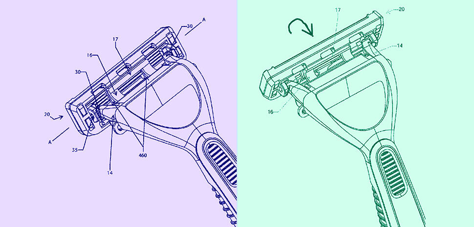
Dallas-Fort Worth ranked No. 9 for patents out of 250 metros. Patents granted include: Astrapi's methods of transmitting data using polynomial-based signals, AT&T's allocation and extraction of data for augmented reality for 6G or other next-gen network, Building Materials Investment Corp.'s moisture sensing roofing systems, COEVAC's automatic smoke/carbon monoxide evacuation system, IBM's cognitive intervention for voice recognition failure, Kioma's child safety seat, SanDisk Technologies' low latency data transfer, Shavelogic's shaving systems, USAA's recommendation engine for cost of a claim, and an unassigned virus immune computer system.
-
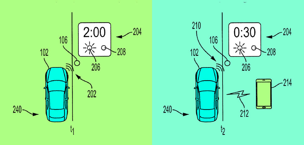
Dallas-Fort Worth ranked No. 11 for patents out of 250 metros. Patents granted include: Bank of America's authentication using blockchains, Dell's validation of data integrity through watermarking, Samsung's compensating for a movement of a sensor attached to a body of a user, SYNERGEN Technology Labs' baby monitor system sound and light delivery based on vitals,Toyota's parking meter monitoring and payment system, and Walmart's product recognition through multi-model image processing.
-
Dallas-Fort Worth ranked No. 11 for patents out of 250 metros. Patents granted include: Allied Bioscience's aqueous antimicrobial coatings, American Leather Operations convertible furniture, Caris Science's method for measuring the amount of at least one molecule in a bio sample, Siemens Industry Software 's environmental perception in autonomous driving STMicroelectronics' NFC antenna switch, Toyota's collaboorative robot hand bearing for high-torque tightening applications, and vSpatial's method for creating a collaborative virtual session.